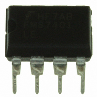
FMS7401LEN Fairchild Semiconductor, FMS7401LEN Datasheet - Page 35

FMS7401LEN
Manufacturer Part Number
FMS7401LEN
Description
IC CTRLR POWER DGTL EEPROM 8DIP
Manufacturer
Fairchild Semiconductor
Datasheet
1.FMS7401LVN.pdf
(81 pages)
Specifications of FMS7401LEN
Applications
Digital Power Controller
Core Processor
8-Bit
Program Memory Type
EEPROM (1 kB)
Ram Size
64 x 8
Number Of I /o
6
Voltage - Supply
2.7 V ~ 3.6 V
Operating Temperature
-40°C ~ 85°C
Mounting Type
Through Hole
Package / Case
8-DIP (0.300", 7.62mm)
Mounting Style
Through Hole
Lead Free Status / RoHS Status
Lead free / RoHS Compliant
Interface
-
Controller Series
-
Lead Free Status / Rohs Status
Lead free / RoHS Compliant
Other names
FMS7401LEN_NL
FMS7401LEN_NL
FMS7401LEN_NL
Available stocks
Company
Part Number
Manufacturer
Quantity
Price
Company:
Part Number:
FMS7401LEN14
Manufacturer:
Rohm
Quantity:
21 626
PRODUCT SPECIFICATION
FMS7401L
Table 15. Dead Time (DTIME) Register Bit Definitions
DTIME Register (addr. 0xA5)
Bit 7
Bit 6
Bit 5
Bit 4
Bit 3
Bit 2
Bit 1
Bit 0
X
X
X
DT[4:0]
DT[4:0]
Dead Time Delay (T
)
DT
0x00
No Dead Time Delay
0x01 – 0x1F
(1/F
) • DT
T1CLK
6.1.3 Timer 1 Control Register
The Timer 1 Control (T1CNTRL) register is used to select Timer 1’s operating mode, enable its PWM output signals, and con-
trol its hardware interrupt (TMRI1). Upon a system reset, the T1CNTRL register is automatically initialized to 0x00. Refer to
Table 16
and
Table 17
for additional details regarding the T1CNTRL register bits.
Bit 7 (T1C3) of the T1CNTRL register selects between the two Timer 1 operating modes. If T1C3=0, the Timer 1 circuit will
be configured in PWM mode. Once Timer 1 is configured in PWM Mode, the TMR1 counter must be started in order for the
circuit to be enabled and considered to be in run mode. If T1C3=1, the Timer 1 circuit will be configured in Input Capture
Mode. Once in Input Capture Mode, the Timer 1 circuit is immediately enabled and the TMR1 counter will automatically
begin incrementing from its initial state (0x000) until Timer 1’s operating mode is returned to a disabled PWM Mode (its
default). Therefore, software must issue a write command clearing T1C3 and T1C0 within the same instruction. If T1C3 is
cleared while T1C0 is set, the Timer 1 circuit will remain in Input Capture Mode until the TMR1 overflows and T
completes
DT
ending the current PWM cycle. Once the TMR1 overflows, the operating mode is switched to a disable PWM Mode even
though T1C0=1. Software must clear T1C0 before re-enabling the Timer 1 circuit in any of the two operating modes.
Bit 6 (T1C2) of the T1CNTRL register has two functions depending on Timer 1’s selected operating mode. In PWM Mode,
T1C2 is used to enable the T1HS2 (G5) output signal (if set). Otherwise, the T1C2 bit (if zero) disables the T1HS2 output sig-
nal. The T1HS2 signal on the G5 pin may be configured as an active high or low output depending on the configured PORTGD
configuration. If PORTGD[5]=0, the T1HS2 (G5) output is active high, otherwise it is active low. In Input Capture Mode,
T1C2 is used to select the edge to trigger a TMR1 T1HS2 input capture. If T1C2=0, every rising edge of the T1HS2 input will
trigger a TMR1 capture. If T1C2=1, every falling edge will trigger a capture. Software may change the value of T1C2 at any
time; however, if the circuit is in run mode, T1C2 will not change the circuit’s attribute until after the TMR1 counter overflows
and the T
passes completing the current PWM cycle. The last T1C2 value after the T
completes, will dictate the circuit’s
DT
DT
attribute for the next PWM cycle. When reading the T1C2, the value reported will be the last value written by software and
may not necessarily reflect the circuit’s attribute for the current PWM cycle.
Bit 5 (T1C1) of the T1CNTRL register enables or disable the T1HS1 (G0) output signal for either operating mode. If T1C1=1,
the T1HS1 output signal is enabled, otherwise it is disabled. The T1HS1 signal on the G0 pin may be configured as an active
high or low output depending on the configured PORTGD configuration. If PORTGD[0]=0, the T1HS1 (G0) output is active
high, otherwise it is active low. Software may change the value of T1C1 at any time; however, if the circuit is in run mode,
T1C1 will not change the circuit’s attribute until after the TMR1 counter overflows and the T
passes completing the current
DT
PWM cycle. The last T1C1 value after the T
completes, will dictate the circuit’s attribute for the next PWM cycle. When
DT
reading the T1C1, the value reported will be the last value written by software and may not necessarily reflect the circuit’s
attribute for the current PWM cycle.
The ADSTROBE signal is outputted through the device’s G1 pin when bit 0 (T1BOUT) of the T1CNTRL register is set
to 1. The ADSTROBE output is always generated by the Timer 1 circuit regardless of the state of T1BOUT. The ADSTROBE
signal on the G1 pin may be configured as an active high or low output depending on the configured PORTGD configuration. If
PORTGD[1]=0, the ADSTROBE (G1) output is active high, otherwise it is active low. Software may change the value of
T1BOUT at any time; however, if the circuit is in run mode, T1BOUT will not change the device’s I/O attribute until after the
TMR1 counter overflows and the T
passes completing the current PWM cycle. The last T1BOUT value after the T
com-
DT
DT
35
REV. 1.0.3 1/24/05


