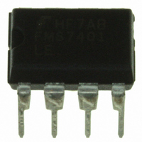
FMS7401LEN Fairchild Semiconductor, FMS7401LEN Datasheet - Page 38

FMS7401LEN
Manufacturer Part Number
FMS7401LEN
Description
IC CTRLR POWER DGTL EEPROM 8DIP
Manufacturer
Fairchild Semiconductor
Datasheet
1.FMS7401LVN.pdf
(81 pages)
Specifications of FMS7401LEN
Applications
Digital Power Controller
Core Processor
8-Bit
Program Memory Type
EEPROM (1 kB)
Ram Size
64 x 8
Number Of I /o
6
Voltage - Supply
2.7 V ~ 3.6 V
Operating Temperature
-40°C ~ 85°C
Mounting Type
Through Hole
Package / Case
8-DIP (0.300", 7.62mm)
Mounting Style
Through Hole
Lead Free Status / RoHS Status
Lead free / RoHS Compliant
Interface
-
Controller Series
-
Lead Free Status / Rohs Status
Lead free / RoHS Compliant
Other names
FMS7401LEN_NL
FMS7401LEN_NL
FMS7401LEN_NL
Available stocks
Company
Part Number
Manufacturer
Quantity
Price
Company:
Part Number:
FMS7401LEN14
Manufacturer:
Rohm
Quantity:
21 626
FMS7401L
The PWM Timer 1 can be programmed to toggle one or both PWM output signals (T1HS1 and T1HS2) to support a variety of
output configurations (half bridge, full bridge,
half-bridge driver and are enabled by programming the T1C1 and T1C2 bits in the T1CNTRL register (see
T1HS1 (G0) and T1HS2 (G5) output signals may be configured with opposite phases and dead time controlled edges (see
Figure
power-up, the T1HS1 and T1HS2 signals may be programmed to default as active high/low outputs by the default I/O configu-
ration register bits in the non-volatile Initialization Register 4.
programmed default state after T
both be configured as outputs with common or opposite phases. If configured as outputs, the PORTGD[0] and PORTGD[5] bits
configure the T1HS1 and T1HS2 signals as active high or low. If the PORTGD bit is 0, the output signal is active high, other-
wise it is active low. The PORTGD[1] bit also configures the G1/ADSTROBE pin as an active high/low signal once configured
as an output. The Initialization Register 4 bits only default the G0/T1HS1 and G5/T1HS2 pins not the G1/ADSTROBE pin.
From factory, the G0/T1HS1, G5/T1HS2 and G1/ADSTROBE device pins are defaulted as tri-stated inputs. The pins must be
configured by the Initialization Register 4 bits or by software directly through the PORTGC and PORTGD register as an output
port before enabling the TMR1 counter and its outputs.
The dead time counter of the Timer 1 circuit controls the dead time (T
transitions through the DT[4:0] bits of the DTIME register. The dead time counter delay is first triggered after the TMR1
counter equals to the T1CMPA value and the T1HS1 signal transitions from its resting (off) to its active (on) state. Once the
programmed T
counter delay is triggered for a second time after the TMR1 counter equals to the T1RA value and the T1HS2 signal transitions
from its active (on) to its resting (off) state. Once the programmed T
active (on) to its resting (off) state ending the PWM cycle. The PWM cycle is considered complete once the TMR1 counter
completes the T1RA count plus T
The T1HS1 and T1HS2 PWM output signals may be programmed to be automatically disabled by the output of the digital filter
(PWMOFF) in Programmable Comparator circuit. The output may be programmed to disable the Timer 1 circuit completely or
disable only the current PWM cycle. Refer to the
The Timer 1’s ADSTROBE output signal may be configured as the G1/ADSTROBE device output if the T1BOUT bit of the
T1CNTRL register is set. The ADSTROBE signal, however, is always generated by the Timer 1 circuit. Initially, the
ADSTROBE begins its PWM cycle at its resting (off) state and transitions to its active (on) state once the TMR1 counter com-
pletes its count equal to the T1CMPB value. The active (on) edge transition of the ADSTROBE output may be programmed to
automatically trigger an ADC conversion cycle if the ENDAS bit of the ADCNTRL2 register is set. Refer to the
section of the datasheet for details.
The T1PND bit of the T1CNTRL register is set once the TMR1 counter completes the count equal to the T1RA value (over-
flows). Software may use the T1PND bit to monitor the PWM cycles and/or trigger microcontroller hardware interrupts
(TMRI1) if the T1EN bit of the T1CNTRL register is set. Software must clear the T1PND bit in order to detect a new overflow
condition and/or trigger a new interrupt.
38
12). The phases of the output signals are configured by the bits of the PORTGD I/O configuration register.
DT
completes, the T1HS2 signal then transitions from its resting (off) to its active (on) state. The dead time
DIO
DT
2
even in the T1HS1 and T1HS2 outputs are disabled.
from the system reset trigger (e.g. from a POR). The G0/T1HS1 and G5/T1HS2 pins may
6
8
low side or high side driving). These outputs may be used to drive an external
Programmable Comparator Circuit
10
Both G0/T1HS1 and G5/T1HS2 pins will configure to their
DT
DT
completes, the T1HS1 signal then transitions from its
) delay between the T1HS1 and T1HS2 output edge
section of the datasheet for details.
PRODUCT SPECIFICATION
REV. 1.0.3 1/24/05
Table
9
ADC Circuit
16). The
Upon device


