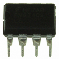
FMS7401LEN Fairchild Semiconductor, FMS7401LEN Datasheet - Page 22

FMS7401LEN
Manufacturer Part Number
FMS7401LEN
Description
IC CTRLR POWER DGTL EEPROM 8DIP
Manufacturer
Fairchild Semiconductor
Datasheet
1.FMS7401LVN.pdf
(81 pages)
Specifications of FMS7401LEN
Applications
Digital Power Controller
Core Processor
8-Bit
Program Memory Type
EEPROM (1 kB)
Ram Size
64 x 8
Number Of I /o
6
Voltage - Supply
2.7 V ~ 3.6 V
Operating Temperature
-40°C ~ 85°C
Mounting Type
Through Hole
Package / Case
8-DIP (0.300", 7.62mm)
Mounting Style
Through Hole
Lead Free Status / RoHS Status
Lead free / RoHS Compliant
Interface
-
Controller Series
-
Lead Free Status / Rohs Status
Lead free / RoHS Compliant
Other names
FMS7401LEN_NL
FMS7401LEN_NL
FMS7401LEN_NL
Available stocks
Company
Part Number
Manufacturer
Quantity
Price
Company:
Part Number:
FMS7401LEN14
Manufacturer:
Rohm
Quantity:
21 626
FMS7401L
this information because the APND bit may be triggered before the ASTART is automatically cleared. The ADC conversion
completion delay may occur when the F
4.2.1 Analog Input Voltage and its 8-bit Digital Result
The relationship between the 8-bit digital value stored in the ADATA register and the analog input voltage is as follows:
• V
• V
4.2.2 ADC Gated Auto-sampling Mode
The ADC circuit may be configured in Gated Auto-sampling Mode by setting the ENDAS bit of the ADCNTRL2 register.
When in Auto-sampling Mode, all ADC conversions are automatically triggered by the active (on) edge transition of the PWM
Timer 1’s ADSTROBE output signal.
time, any triggers issued while a conversion is in progress (ASTART=1) are ignored. Once the trigger is detected, the ASTART
bit of the ADCNTRL1 register is set symbolizing that a conversion is in progress. The initial conversion phase, the sample and
hold or autozero (if GAIN=1), begins after a 1µS cycle delay.
ADATA register, the APND flag is set to trigger a hardware interrupt (if enabled) flagging software that the ADATA register has
been updated with the ADC conversion results. Once all phases of the ADC conversion cycle completes, the ASTART bit is
then automatically cleared by the ADC circuit. Since software cannot change the ADC circuit configuration while an ADC con-
version is in progress, the ASTART bit must be monitored to determine when the conversion cycle completes. Software cannot
rely on the APND bit for this information because the APND bit may be triggered before the ASTART is automatically cleared.
The ADC conversion completion delay may occur when the F
4.2.3 ADC Conversion Clock Configuration
The ADC conversion clock (F
1’s clock (F
circuit is automatically configured to source the F
is selected, the ADC circuit is automatically configured to source the F
conversions with the active (on) edge of the PWM Timer 1 ADSTROBE output signal.
When in standard ADC conversion mode, the ASPEED[1:0] bits of the ADCNTRL2 register may be used to slow the total con-
version time improving the ADC conversion accuracy. However, if the F
FMODE=1) the F
then be divided by setting the ASPEED[1:0]=3 divide factor to yield a F
may temporarily clear FMODE returning the conversion cycle to its proper frequency and free the ASPEED bits to be used to
improve the conversion accuracy. In addition, if the internal oscillator is trimmed to its upper F
the F
divide factor may still be selected by setting the ASPEED[1:0]>1.
When in ADC Conversion Auto-sampling Mode, the ADC circuit automatically configures the F
the F
ever, the F
needed to yield the proper F
are evaluated so that the divide circuit applies the appropriate divide factor to the F
ASPEED[1:0] bits of the ADCNTRL2 register may be used to slow the total conversion time improving the ADC conversion
22
V
ADC
ADC
ACH(x)
ICLK
T1CLK
=
is the 8-bit digital result of an ADC conversion.
V
-------------------- -
clock, the ASPEED[1:0]=1 divided factor must be selected to yield a F
V
T1CLK
is the analog voltage applied to the selected input channel.
ACH x ( )
clock so that the ADC conversions may be synchronized with the active (on) edge of the ADSTROBE signal. How-
T1CLK
AREF
clock is first sent into a special divide circuit which evaluates its configuration to determine the divide factor
) depending on the ADC circuit’s operating mode. If the standard ADC conversion mode is selected, the ADC
ADCLK
×
255
will clock eight times faster than the proper conversion rate (1µS cycle time). The F
ADCLK
ADCLK
conversion rate (1µS cycle time). The FMODE, FSEL, and FS bits of the PSCALE register
) is sourced either by the device’s main system instruction clock (F
2
If the period of the PWM ADSTROBE signal is less than the total ADC conversion
ICLK
clock is slower than an ADC conversion clock cycle.
ADCLK
clock by the F
7
ICLK
Once all eight digital bits are determined and stored in the
clock is slower than an ADC conversion clock cycle.
ADCLK
ICLK
ICLK
ADCLK
clock. If the ADC Conversion Auto-sampling Mode
clock by the F
clock is sourced by the PLL’s F
/8 conversion clock cycle. Otherwise, software
ADCLK
T1CLK
/2 conversion clock cycle.
2
clock (the PS bits do not apply). The
T1CLK
OSC
clock to synchronize the ADC
ADCLK
frequency and it is sourcing
PRODUCT SPECIFICATION
ICLK
clock to be sourced by
) or the PWM Timer
REV. 1.0.3 1/24/05
(FS=0)
ADCLK
8
output (when
A greater
clock must


