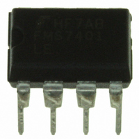
FMS7401LEN Fairchild Semiconductor, FMS7401LEN Datasheet - Page 23

FMS7401LEN
Manufacturer Part Number
FMS7401LEN
Description
IC CTRLR POWER DGTL EEPROM 8DIP
Manufacturer
Fairchild Semiconductor
Datasheet
1.FMS7401LVN.pdf
(81 pages)
Specifications of FMS7401LEN
Applications
Digital Power Controller
Core Processor
8-Bit
Program Memory Type
EEPROM (1 kB)
Ram Size
64 x 8
Number Of I /o
6
Voltage - Supply
2.7 V ~ 3.6 V
Operating Temperature
-40°C ~ 85°C
Mounting Type
Through Hole
Package / Case
8-DIP (0.300", 7.62mm)
Mounting Style
Through Hole
Lead Free Status / RoHS Status
Lead free / RoHS Compliant
Interface
-
Controller Series
-
Lead Free Status / Rohs Status
Lead free / RoHS Compliant
Other names
FMS7401LEN_NL
FMS7401LEN_NL
FMS7401LEN_NL
Available stocks
Company
Part Number
Manufacturer
Quantity
Price
Company:
Part Number:
FMS7401LEN14
Manufacturer:
Rohm
Quantity:
21 626
accuracy. However, if the internal oscillator is trimmed to its upper F
ASPEED[1:0]=1 divided factor must be selected to yield a F
be selected by setting the ASPEED[1:0]>1.
4.3
The GAIN bit of the ADCNTRL2 register enables the Autozero Amplifier circuit. To perform a proper ADC conversion using
the autozero amplifier, software must configure its non-inverting input (G4/AIN0) as a tri-state input bypassing the I/O
circuitry. The autozero amplifier has a gain of 16, but is not defined as a true differential amplifier because the inverting
SR_GND input must be connected as close to ground as possible (e.g. to act as a Kelvin connection) to reduce noise and
improve the precision of the measurement.
To perform an ADC conversion through the autozero amplifier, the ACH1 input channel of the analog mux must be selected.
The autozero ADC conversion is divided in three phases lasting a total of 20 conversion clock cycles. In the first phase, occu-
pying the first six conversion cycles, it calculates the offset voltage of the amplifier. The second phase, occupying the next five
cycles, adds or subtracts the offset voltage to the amplified input voltage which now has a gain of 16. The final phase, occupy-
ing the last nine cycles, converts the autozero input voltage to an 8-bit digital value and stores it in the ADATA register for easy
access by software.
4.4
The Uncommitted Amplifier Enable (ENAMP) bit of the ADCNTRL2 register enables the Uncommitted Amplifier (AMP)
circuit whose inverting input is connected to the G6/-A
circuit, software must configure both the G6/-A
AMP circuit may be used in any control or battery management applications.
In control applications, the AMP circuit is used as the error amplifier in a hardware closed loop whose input connections are
part of the external compensation loop circuit. The output of the amplifier (A
Comparator circuit to control the PWM T1HS1 and T1HS2 inputs of the control plant block. An ADC conversion may be
triggered to monitor A
The AMP circuit may be configured as a general uncommitted amplifier whose non-inverting input is connected to V
Therefore, the AMP circuit may only amplify differences with respect to V
vert the voltage at A
circuit may be used to improve the resolution of the battery voltage measurement by adding a gain through the feedback loop.
Voltage variation at a typical point will be amplified with a gain for better resolution, for example, to sense the Negative Delta
V (NDV) to determine the end of change for a NiCD or NiMH battery.
4.5
The Current Source Enable (ENIS) bit of the ADCNTRL2 register enables the Current Source Generator (ISOURCE) circuit
connected to the G3/AIN1 pin. Before enabling the ISOURCE circuit, software must configure the G3/AIN1 port as a tri-state
input bypassing all I/O circuitry.
used to interface to an opto-coupler output.
voltage developed at the G3/AIN1 input can be converted by the ADC circuit if the ACH2 analog input channel is selected.
The ISOURCE and ADC circuit combination may also be used to measure Capacitive Sensors or the resistance of a thermistor
(NTC/PTC) to indirectly measure the temperature.
REV. 1.0.3 1/24/05
PRODUCT SPECIFICATION
Autozero Amplifier
Uncommitted Amplifier
Current Source Generator
OUT
OUT
by selecting the ACH5 input channel of the analog mux. In battery management applications, the AMP
by selecting the ACH5 input channel of the analog mux.
9
Once the ENIS bit is set, the ISOURCE circuit begins to generate I
1
Figure 7
IN
and G7/A
provides an example of a typical ISOURCE application where the
IN
and output to the G7/A
OUT
ADCLK
pins as tri-state input ports bypassing all I/O circuitry. The
/2 conversion clock cycle.
OSC
frequency while FMODE and FSEL are zero, the
REF
OUT
. An ADC conversion may be triggered to con-
OUT
) is internally fed to the Programmable
port pins. Before enabling the AMP
8
A greater divide factor may still
SRC
of current typically
FMS7401L
REF
.
23


