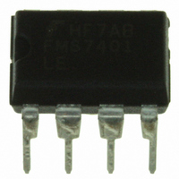
FMS7401LEN Fairchild Semiconductor, FMS7401LEN Datasheet - Page 37

FMS7401LEN
Manufacturer Part Number
FMS7401LEN
Description
IC CTRLR POWER DGTL EEPROM 8DIP
Manufacturer
Fairchild Semiconductor
Datasheet
1.FMS7401LVN.pdf
(81 pages)
Specifications of FMS7401LEN
Applications
Digital Power Controller
Core Processor
8-Bit
Program Memory Type
EEPROM (1 kB)
Ram Size
64 x 8
Number Of I /o
6
Voltage - Supply
2.7 V ~ 3.6 V
Operating Temperature
-40°C ~ 85°C
Mounting Type
Through Hole
Package / Case
8-DIP (0.300", 7.62mm)
Mounting Style
Through Hole
Lead Free Status / RoHS Status
Lead free / RoHS Compliant
Interface
-
Controller Series
-
Lead Free Status / Rohs Status
Lead free / RoHS Compliant
Other names
FMS7401LEN_NL
FMS7401LEN_NL
FMS7401LEN_NL
Available stocks
Company
Part Number
Manufacturer
Quantity
Price
Company:
Part Number:
FMS7401LEN14
Manufacturer:
Rohm
Quantity:
21 626
Table 16. Timer 1 Control (T1CNTRL) Register Bit Definitions
Table 17. Timer 1 Mode Configuration Bits
6.2
In PWM Mode, the Timer 1 circuit may be configured to generate pulses of a specified duty cycle and period on the T1HS1
(G0), T1HS2 (G5), and/or ADSTROBE (G1) timer outputs. The 12-bit TMR1 counter increments at the F
defined by the FSEL bit of the PSCALE register. Refer to the previous
section
A PWM cycle begins with the TMR1 counter incrementing from 0x000 until it matches the value stored in the T1RA register.
At this point, the TMR1 counter completes its T1RA count and overflows (a transitions from T1RA to 0x000) setting the
T1PND flag of the T1CNTRL register ending the PWM cycle. The Timer 1 circuit has two additional TMR1 compare
(T1CMPA and T1CMPB) registers used to generate the T1HS1, T1HS2, and ADSTROBE output signals. All three output
signals are initialized to a resting (off) state. Once the TMR1 counter is enabled (by setting the T1C0 bit of the T1CNTRL
register), both compare registers are matched against the incrementing TMR1 counter. When the TMR1 completes its count
equal to the value stored in the T1CMPA and T1CMPB registers, the T1HS1, T1HS2, and ADSTROBE output signals are set
to an active (on) state until the TMR1 counter matches the value stored in the T1RA compare register (overflows). Once the
TMR1 counter overflows, the output signals are cleared returning them to a resting (off) state. Refer to
PWM Mode block diagram.
REV. 1.0.3 1/24/05
PRODUCT SPECIFICATION
Bit
T1C3
T1C2
T1C1
T1C0
T1PND
T1EN
T1BOUT
T1C3
0
0
0
0
1
1
1
1
T1C3
Bit 7
Pulse Width Modulation (PWM) Mode
of the datasheet for details.
T1C2
0
1
0
1
0
0
1
1
Description
Timer 1 Mode Configuration Bit. Refer to
Timer 1 Mode Configuration Bit. Refer to
Timer 1 Mode Configuration Bit. Refer to
PWM Mode
(0) Stop the PWM Timer 1 circuit.
(1) Start the PWM Timer 1 circuit.
Input Capture Mode
(0) Timer 1’s TMR1 overflow pending flag is cleared.
(1) Timer 1’s TMR1 overflow pending flag is triggered.
PWM Mode
(0) Timer 1’s TMR1 overflow pending flag is cleared.
(1) Timer 1’s TMR1 overflow pending flag is triggered.
Input Capture Mode
(0) Timer 1 capture pending flag is cleared.
(1) Timer 1 capture pending flag is triggered.
(0) Disables Timer 1 hardware interrupts.
(1) Enables Timer 1 hardware interrupts.
(0) Retain normal I/O function of the G1/AIN3 pin.
(1) Enables Timer 1’s ADSTROBE output to be sent to the G1 output port.
T1C1
T1C2
0
1
1
0
0
1
0
1
Bit 6
PWM mode no output toggle
PWM mode T1HS1 and T1HS2 toggle
PWM mode T1HS1 toggle
PWM mode T1HS2 toggle
Capture mode no T1HS1 toggle
Capture mode with T1HS1 toggle
Capture mode no T1HS1 toggle
Capture mode with T1HS1 toggle
T1C1
Bit 5
Timer Mode Source
T1CNTRL Register (addr. 0xAE)
T1C0
Bit 4
Table 17
Table 17
Table 17
for details.
for details.
for details.
T1PND
Bit 3
PSCALE Register and Timer 1 Clock Configuration
T1HS2 falling-edge
T1HS2 falling-edge
T1HS2 rising-edge
T1HS2 rising-edge
TMR1 Overflow
TMR1 Overflow
TMR1 Overflow
TMR1 Overflow
TMR1 Overflow
TMR1 Overflow
TMR1 Overflow
TMR1 Overflow
Interrupt
T1EN
Bit 2
Bit 1
X
Figure 11
T1CLK
Timer count on
Prescaler Input
Prescaler Input
Prescaler Input
Prescaler Input
Prescaler Input
Prescaler Input
Prescaler Input
Prescaler Input
clock rate
for a Timer 1
T1BOUT
Bit 0
FMS7401L
37


