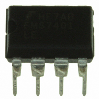
FMS7401LEN Fairchild Semiconductor, FMS7401LEN Datasheet - Page 19

FMS7401LEN
Manufacturer Part Number
FMS7401LEN
Description
IC CTRLR POWER DGTL EEPROM 8DIP
Manufacturer
Fairchild Semiconductor
Datasheet
1.FMS7401LVN.pdf
(81 pages)
Specifications of FMS7401LEN
Applications
Digital Power Controller
Core Processor
8-Bit
Program Memory Type
EEPROM (1 kB)
Ram Size
64 x 8
Number Of I /o
6
Voltage - Supply
2.7 V ~ 3.6 V
Operating Temperature
-40°C ~ 85°C
Mounting Type
Through Hole
Package / Case
8-DIP (0.300", 7.62mm)
Mounting Style
Through Hole
Lead Free Status / RoHS Status
Lead free / RoHS Compliant
Interface
-
Controller Series
-
Lead Free Status / Rohs Status
Lead free / RoHS Compliant
Other names
FMS7401LEN_NL
FMS7401LEN_NL
FMS7401LEN_NL
Available stocks
Company
Part Number
Manufacturer
Quantity
Price
Company:
Part Number:
FMS7401LEN14
Manufacturer:
Rohm
Quantity:
21 626
Table 5. ADCNTRL1 Register Bit Definitions
Table 6. Analog Input Channel Selection (ACHSEL[3:0]) Bit Definitions
4.1.2 ADCNTRL2 Register
The ADCNTRL2 is an 8-bit memory map register used to configure the analog circuits. Six of the eight register bits are used to
configure circuits directly related to the ADC circuit while the others are not related.
Bit 7 (REFBY2) of the ADCNTRL2 register is the reference clock (F
ures the reference clock of the PLL and Programmable Comparator circuit to be sourced either by F
Refer to the
Bit 6 (COMPSEL) of the ADCNTRL2 register is the Programmable Comparator’s non-inverting input selection bit. If
COMPSEL=0, the non-inverting input of the Programmable Comparator is the G4/AIN0 device pin. If COMPSEL=1, the
non-inverting input of the Programmable Comparator is the G2/AIN2 device pin. Before enabling the Programmable
Comparator circuit, the selected analog input port pin must be configured as a tri-state input bypassing the I/O circuitry.
Refer to the
Bit 5 of the ADCNTRL2 register is the Uncommitted Amplifier Enable (ENAMP) bit. If ENAMP=0, the Uncommitted Ampli-
fier circuit is disabled and its pin connections (G6/-A
still be used as a standard ADC conversion input through the analog ACH5 channel. If ENAMP=1, the Uncommitted Amplifier
circuit is enabled and its pin connections must be configured as tri-state inputs where G6/-A
A
Uncommitted Amplifier, software must avoid clearing the ENAMP bit. Refer to the following
for additional details.
Bit 4 (ENDAS) of the ADCNTRL2 register enables the ADC conversion’s gated auto-sampling operating mode. If ENDAS=1,
the ADC circuit configures the F
ADC circuit will then accept triggers by the active (on) edge transition of the ADSTROBE signal. All other ADC configuration
REV. 1.0.3 1/24/05
PRODUCT SPECIFICATION
Bit
APND
AINTEN
ASTART
REFSEL
ACHSEL[3:0]
OUT
APND
ACHSEL[3]
Bit 7
is the amplifier output.
0
0
0
0
1
1
1
1
Clock Circuit
Programmable Comparator Circuit
AINTEN
Bit 6
ACHSEL[2]
section of the datasheet for additional details.
9
If the ADC circuit is performing a conversion on the analog ACH5 input when driven by the
0
0
0
0
0
0
0
1
ADCLK
Description
(0) ADC’s pending flag is cleared.
(1) ADC’s pending flag is triggered.
(0) Disables ADC hardware interrupts.
(1) Enables ADC hardware interrupts.
(0) ADC conversion is not in progress.
(1) Start an ADC conversion / ADC conversion in progress.
(0) ADC Reference (V
(1) ADC Reference (V
Analog Input Channel Selection Bits. Refer to
ASTART
Bit 5
clock for synchronization with the PWM Timer 1’s ADSTROBE output signal. The
ACHSEL[1]
ADCNTRL1 Register (addr. 0x9F)
section of the datasheet for addition details.
REFSEL
0
0
1
1
0
0
1
0
AREF
AREF
IN
Bit 4
and G7/A
) = Internal V
) = Vcc
OUT
REF
ACHSEL[0]
) may be used as normal I/O ports. The G7/AIN4 pin may
Bit 3
RCLK1
0
1
0
1
0
1
0
0
Table 6
) divide-by-2 enable bit. The REFBY2 bit config-
for details.
Bit 2
Analog Channel
ACHSEL[3:0]
ACH1
ACH2
ACH3
ACH4
ACH5
+V
Vcc/3
IN
GND
Uncommitted Amplifier
REF
is the inverting input and G7/
RCLK1
Bit 1
or F
G7/AIN4/A
RCLK1
I/O Equiv.
G4/AIN0
G3/AIN1
G2/AIN2
G1/AIN3
-
-
-
/2 clock.
Bit 0
FMS7401L
section
OUT
9
19


