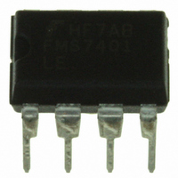
FMS7401LEN Fairchild Semiconductor, FMS7401LEN Datasheet - Page 25

FMS7401LEN
Manufacturer Part Number
FMS7401LEN
Description
IC CTRLR POWER DGTL EEPROM 8DIP
Manufacturer
Fairchild Semiconductor
Datasheet
1.FMS7401LVN.pdf
(81 pages)
Specifications of FMS7401LEN
Applications
Digital Power Controller
Core Processor
8-Bit
Program Memory Type
EEPROM (1 kB)
Ram Size
64 x 8
Number Of I /o
6
Voltage - Supply
2.7 V ~ 3.6 V
Operating Temperature
-40°C ~ 85°C
Mounting Type
Through Hole
Package / Case
8-DIP (0.300", 7.62mm)
Mounting Style
Through Hole
Lead Free Status / RoHS Status
Lead free / RoHS Compliant
Interface
-
Controller Series
-
Lead Free Status / Rohs Status
Lead free / RoHS Compliant
Other names
FMS7401LEN_NL
FMS7401LEN_NL
FMS7401LEN_NL
Available stocks
Company
Part Number
Manufacturer
Quantity
Price
Company:
Part Number:
FMS7401LEN14
Manufacturer:
Rohm
Quantity:
21 626
5
The Programmable Comparator circuit is an analog comparator whose outputs may be monitored by software or fed into a dig-
ital delay filter used to disable the PWM Timer 1 circuit or its PWM cycle. The comparator’s non-inverting input is software
selectable by the COMPSEL bit of the ADCNTRL2 register.
Comparator is the G4/AIN0 device pin. If COMPSEL=1, the non-inverting input of the Programmable Comparator is the G2/
AIN2 device pin. Before enabling the Programmable Comparator circuit, the selected analog input port pin must be configured
as a tri-state input bypassing the I/O circuitry.
(VLOOP) enable bit of the comparator control (COMP) register. If VLOOP=0, the voltage loop is disabled and the inverting
input of the analog comparator is configured as one of the 63 programmable voltage levels (V
analog comparator is set in a voltage loop configuration with the Uncommitted (Error) Amplifier output (A
the comparator’s inverting input (see
The Programmable Comparator circuit may be configured and controlled by software through the two 8-bit Comparator
Control (COMP) and Digital Delay (DDELAY) registers. Both the Programmable Comparator and the digital delay filter
must be enabled by software by setting the Comparator Enable (COMPEN) and clearing the EPWM bits of the Digital Delay
(DDELAY) register. Upon a system reset, the Programmable Comparator is disabled and the digital delay filter is enabled.
The COMP circuit is automatically disabled during Halt Mode. After exiting the Halt Mode, software must wait at least 10
instruction clock cycles before reading the COUT bit to ensure that the internal circuit has stabilized.
Table 8. Programmable Comparator (COMP) Control Register Bit Definitions
5.1
The Programmable Comparator circuit is configured to compare the G4/AIN0 or G2/AIN2 non-inverting input against the pro-
grammable voltage threshold levels on its inverting input (see
the G4/AIN0 or G2/AIN2 input pin rises above the selected voltage threshold. As long as the input stays above the selected
voltage threshold, the C
falls below the programmed threshold voltage or if the Programmable Comparator circuit is disabled. Software may change the
programmed threshold voltage on-the-fly as needed in the application. If the digital delay filter circuit is enabled (EPWM=0),
the C
Delay Filter with PWMOFF Output
Bit 6 of the ADCNTRL2 register is the Programmable Comparator non-inverting input selection (COMPSEL) bit.
COMPSEL=0, the non-inverting input of the Programmable Comparator is the G4/AIN0 device pin. If COMPSEL=1, the non-
inverting input of the Programmable Comparator is the G2/AIN2 device pin. Before enabling the Programmable Comparator
circuit, the selected analog input port pin must be configured as a tri-state input bypassing the I/O circuitry.
REV. 1.0.3 1/24/05
PRODUCT SPECIFICATION
Bit
CL[5:0]
VLOOP
COUT
OUT
Programmable Comparator Circuit
Bit 7
Programmable Comparator’s Voltage Threshold Levels (VLOOP=0)
signal is monitored for its rising edge to generate the PWMOFF signal. Refer to
Description
Programmable Comparator Voltage Reference Level bits. Refer to
(0) Configures the inverting input of the analog comparator as one of the 63 programmable voltage levels (V
(1) Configures the analog comparator in a voltage loop configuration with the Uncommitted Amplifier output (A
connected to the inverting input.
(0) G2/AIN2 or G4/AIN0 non-inverting input is less than inverting input configured by VLOOP.
(1) G2/AIN2 or G4/AIN0 non-inverting input is greater than inverting input configured by VLOOP.
Bit 6
OUT
signal will hold its state. The C
section for addition details.
Bit 5
Figure
CL[5:0]
9).
2
The inverting input of the comparator is controlled by the Voltage Loop
COMP Register (addr. 0xA0)
Bit 4
OUT
1
If COMPSEL=0, the non-inverting input of the Programmable
Table 9
signal will equal zero if the G4/AIN0 or G2/AIN2 input voltage
Bit 3
and
Table
Table 9
10). The comparator output (C
and
Bit 2
Table 10
Figure 8
THL
for details.
, V
VLOOP
and the following
THU
Bit 1
). If VLOOP=1, the
OUT
2
) connected to
OUT
THL
1
OUT
) is 1 when
COUT
, V
If
Bit 0
FMS7401L
Digital
)
THU
).
25


