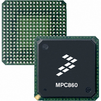
MC68MH360ZP33L Freescale Semiconductor, MC68MH360ZP33L Datasheet - Page 102

MC68MH360ZP33L
Manufacturer Part Number
MC68MH360ZP33L
Description
IC MPU 32BIT QUICC 357-PBGA
Manufacturer
Freescale Semiconductor
Specifications of MC68MH360ZP33L
Processor Type
M683xx 32-Bit
Speed
33MHz
Voltage
5V
Mounting Type
Surface Mount
Package / Case
357-PBGA
Lead Free Status / RoHS Status
Contains lead / RoHS non-compliant
Features
-
Available stocks
Company
Part Number
Manufacturer
Quantity
Price
Company:
Part Number:
MC68MH360ZP33L
Manufacturer:
FREESCALE
Quantity:
1 831
Company:
Part Number:
MC68MH360ZP33L
Manufacturer:
MOTOLOLA
Quantity:
672
Company:
Part Number:
MC68MH360ZP33L
Manufacturer:
Freescale Semiconductor
Quantity:
10 000
Part Number:
MC68MH360ZP33L
Manufacturer:
FREESCALE
Quantity:
20 000
Company:
Part Number:
MC68MH360ZP33LR2
Manufacturer:
Freescale Semiconductor
Quantity:
10 000
- Current page: 102 of 962
- Download datasheet (5Mb)
Bus Operation
State 1—One-half clock later, in state 1 (S1), the QUICC asserts AS indicating a valid
address on the address bus. The QUICC also asserts DS and OE during S1. The selected
device uses R/W, SIZ1 or SIZ0, A0, A1, DS, and OE to place its information on the data bus.
Any or all of the bytes (D31–D24, D23–D16, D15–D8, and D7–D0) are selected by SIZ1,
SIZ0, A1, and A0. Concurrently, the selected device asserts DSACKx.
State 2—As long as at least one of the DSACKx signals is recognized on the falling edge of
S2 (meeting the asynchronous input setup time requirement), data is latched on the falling
edge of S4, and the cycle terminates.
State 3—If DSACKx is not recognized by the start of state 3 (S3), the QUICC inserts wait
states instead of proceeding to states 4 and 5. To ensure that wait states are inserted, both
DSACK1 and DSACK0 must remain negated throughout the asynchronous input setup and
hold times around the end of S2. If wait states are added, the QUICC continues to sample
DSACKx on the falling edges of the clock until one is recognized.
State 4—At the falling edge of state 4 (S4), the QUICC latches the incoming data and sam-
ples DSACKx to get the port size.
State 5—The QUICC negates AS, DS, and OE during state 5 (S5). It holds the address valid
during S5 to provide address hold time for memory systems. R/W, SIZ1, SIZ0, and FC3–
FC0 also remain valid throughout S5. The external device keeps its data and DSACKx sig-
nals asserted until it detects the negation of AS, DS, or OE (whichever it detects first). The
device must remove its data and negate DSACKx within approximately one clock period
after sensing the negation of AS, DS, or OE. DSACKx signals that remain asserted beyond
this limit may be prematurely detected for the next bus cycle.
4.3.2 Write Cycle
During a write cycle, the QUICC transfers data to memory or a peripheral device. Figure 4-
19 is a flowchart of a write cycle operation for a long-word transfer. Figure 4-20 shows the
functional write cycle timing diagram specified in clock periods for two write cycles (between
two read cycles with no idle time) for a 32-bit port.
4-26
1) SET R/W TO WRITE
2) DRIVE ADDRESS ON A31–A0
3) DRIVE FUNCTION CODE ON FC3–FC0
4) DRIVE SIZE (SIZ1–SIZ0)
5) ASSERT ADDRESS STROBE (AS) AND WEx
6) DRIVE DATA LINES D31–D0
7) ASSERT DATA STROBE (DS)
1) NEGATE AS AND DS AND WEx
2) REMOVE DATA FROM D31–D0
START NEXT CYCLE
ADDRESS DEVICE
ACQUIRE DATA
PROCESSOR
Freescale Semiconductor, Inc.
Figure 4-19. Write Cycle Flowchart
For More Information On This Product,
MC68360 USER’S MANUAL
Go to: www.freescale.com
1) DECODE ADDRESS
2) PLACE DATA ON D31–D0
3) ASSERT DATA TRANSFER AND SIZE
1) NEGATE DSACKx
ACKNOWLEDGE (DSACKx)
EXTERNAL DEVICE
TERMINATE CYCLE
PRESENT DATA
MOTOROLA
Related parts for MC68MH360ZP33L
Image
Part Number
Description
Manufacturer
Datasheet
Request
R
Part Number:
Description:
Manufacturer:
Freescale Semiconductor, Inc
Datasheet:
Part Number:
Description:
Manufacturer:
Freescale Semiconductor, Inc
Datasheet:
Part Number:
Description:
Manufacturer:
Freescale Semiconductor, Inc
Datasheet:
Part Number:
Description:
Manufacturer:
Freescale Semiconductor, Inc
Datasheet:
Part Number:
Description:
Manufacturer:
Freescale Semiconductor, Inc
Datasheet:
Part Number:
Description:
Manufacturer:
Freescale Semiconductor, Inc
Datasheet:
Part Number:
Description:
Manufacturer:
Freescale Semiconductor, Inc
Datasheet:
Part Number:
Description:
Manufacturer:
Freescale Semiconductor, Inc
Datasheet:
Part Number:
Description:
Manufacturer:
Freescale Semiconductor, Inc
Datasheet:
Part Number:
Description:
Manufacturer:
Freescale Semiconductor, Inc
Datasheet:
Part Number:
Description:
Manufacturer:
Freescale Semiconductor, Inc
Datasheet:
Part Number:
Description:
Manufacturer:
Freescale Semiconductor, Inc
Datasheet:
Part Number:
Description:
Manufacturer:
Freescale Semiconductor, Inc
Datasheet:
Part Number:
Description:
Manufacturer:
Freescale Semiconductor, Inc
Datasheet:
Part Number:
Description:
Manufacturer:
Freescale Semiconductor, Inc
Datasheet:


