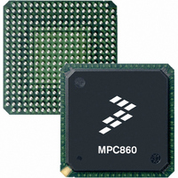
MC68MH360ZP33L Freescale Semiconductor, MC68MH360ZP33L Datasheet - Page 294

MC68MH360ZP33L
Manufacturer Part Number
MC68MH360ZP33L
Description
IC MPU 32BIT QUICC 357-PBGA
Manufacturer
Freescale Semiconductor
Specifications of MC68MH360ZP33L
Processor Type
M683xx 32-Bit
Speed
33MHz
Voltage
5V
Mounting Type
Surface Mount
Package / Case
357-PBGA
Lead Free Status / RoHS Status
Contains lead / RoHS non-compliant
Features
-
Available stocks
Company
Part Number
Manufacturer
Quantity
Price
Company:
Part Number:
MC68MH360ZP33L
Manufacturer:
FREESCALE
Quantity:
1 831
Company:
Part Number:
MC68MH360ZP33L
Manufacturer:
MOTOLOLA
Quantity:
672
Company:
Part Number:
MC68MH360ZP33L
Manufacturer:
Freescale Semiconductor
Quantity:
10 000
Part Number:
MC68MH360ZP33L
Manufacturer:
FREESCALE
Quantity:
20 000
Company:
Part Number:
MC68MH360ZP33LR2
Manufacturer:
Freescale Semiconductor
Quantity:
10 000
- Current page: 294 of 962
- Download datasheet (5Mb)
System Integration Module (SIM60)
Bit 5—PWW
Bit 4—CAS2, CAS3/IACK3, IACK6
Bit 2—CAS0, CAS1/IACK1, IACK2
Bit 1—CS7/IACK7
Bit 0—AVEC (AVECO)/IACK5
6.10 MEMORY CONTROLLER
The memory controller is a sub-block of the SIM60 that is responsible for up to eight general-
purpose chip-select lines and the DRAM controller. The DRAM controller itself can control
up to eight memory banks.
6.10.1 Memory Controller Key Features
The key features of the memory controller are as follows:
6-50
This read-only bit is used to indicate if the WE/ADDR and the PRTY lines have been pro-
grammed by the user or are still in the three-state condition because the PEPAR register
has not been written.
• All Eight Memory Banks Support the Following:
0 = PEPAR has not been written. The WE/ADDR and the PRTY lines are still being
1 = PEPAR was written. The WE/ADDR and the PRTY lines have been programmed
0 = The CAS2 and CAS3 output functions are selected.
1 = The IACK3 and IACK6 output functions are selected.
0 = The CAS0 and CAS1 output functions are selected.
1 = The IACK1 and IACK2 output functions are selected.
0 = The CS7 output function is selected.
1 = The IACK7 output function is selected.
0 = The AVEC input function is selected in normal operation, or AVECO is selected in
1 = The IACK5 output function is selected.
—32-Bit Address Decode with 17 Bits of Address Masking
—Various Block Sizes—2 Kbytes up to 256 Mbytes
—From 0 to 15 Wait States Programmable with DSACK Generation
—Memory Bank Can Be Used by an External Master
—Supports Burst Accesses of the MC68040
—Byte Parity Generation/Checking
—Write-Protect Capability
—Four Byte-Write Enable (WE) Signals
—Output Enable (OE) Signal
—Special Options for Interfacing to Slow Peripherals
—Function Code Match with Mask Can Qualify Memory Bank Accesses
three-stated.
in the PEPAR, so the configuration choices of these pins in the PEPAR are valid.
slave mode.
Freescale Semiconductor, Inc.
For More Information On This Product,
MC68360 USER’S MANUAL
Go to: www.freescale.com
MOTOROLA
Related parts for MC68MH360ZP33L
Image
Part Number
Description
Manufacturer
Datasheet
Request
R
Part Number:
Description:
Manufacturer:
Freescale Semiconductor, Inc
Datasheet:
Part Number:
Description:
Manufacturer:
Freescale Semiconductor, Inc
Datasheet:
Part Number:
Description:
Manufacturer:
Freescale Semiconductor, Inc
Datasheet:
Part Number:
Description:
Manufacturer:
Freescale Semiconductor, Inc
Datasheet:
Part Number:
Description:
Manufacturer:
Freescale Semiconductor, Inc
Datasheet:
Part Number:
Description:
Manufacturer:
Freescale Semiconductor, Inc
Datasheet:
Part Number:
Description:
Manufacturer:
Freescale Semiconductor, Inc
Datasheet:
Part Number:
Description:
Manufacturer:
Freescale Semiconductor, Inc
Datasheet:
Part Number:
Description:
Manufacturer:
Freescale Semiconductor, Inc
Datasheet:
Part Number:
Description:
Manufacturer:
Freescale Semiconductor, Inc
Datasheet:
Part Number:
Description:
Manufacturer:
Freescale Semiconductor, Inc
Datasheet:
Part Number:
Description:
Manufacturer:
Freescale Semiconductor, Inc
Datasheet:
Part Number:
Description:
Manufacturer:
Freescale Semiconductor, Inc
Datasheet:
Part Number:
Description:
Manufacturer:
Freescale Semiconductor, Inc
Datasheet:
Part Number:
Description:
Manufacturer:
Freescale Semiconductor, Inc
Datasheet:


