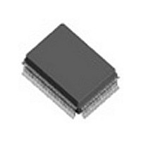
IDT82V2108PXG8 IDT, Integrated Device Technology Inc, IDT82V2108PXG8 Datasheet - Page 57

IDT82V2108PXG8
Manufacturer Part Number
IDT82V2108PXG8
Description
IC FRAMER T1/J1/E1 8CH 128-PQFP
Manufacturer
IDT, Integrated Device Technology Inc
Datasheet
1.IDT82V2108PX8.pdf
(292 pages)
Specifications of IDT82V2108PXG8
Controller Type
T1/E1/J1 Framer
Interface
Parallel
Voltage - Supply
2.97 V ~ 3.63 V
Current - Supply
160mA
Operating Temperature
-40°C ~ 85°C
Mounting Type
Surface Mount
Package / Case
128-MQFP, 128-PQFP
Screening Level
Industrial
Mounting
Surface Mount
Operating Temperature (min)
-40C
Operating Temperature (max)
85C
Lead Free Status / RoHS Status
Lead free / RoHS Compliant
Other names
82V2108PXG8
Available stocks
Company
Part Number
Manufacturer
Quantity
Price
Company:
Part Number:
IDT82V2108PXG8
Manufacturer:
IDT, Integrated Device Technology Inc
Quantity:
10 000
- Current page: 57 of 292
- Download datasheet (3Mb)
IDT82V2108
3.11.2.1.2
clocked by RSCCK. The active edge of RSCCK to sample the pulse on
RSCFS or to update the data on the RSDn, RSFSn and RSSIGn pins is
determined by the following bits in the registers (refer to Table 23).
each channel is the first bit to be output.
Slave mode, the special feature in this mode is that the multi-functional
pin RSCKn/RSSIGn is used as RSSIGn to output the extracted signaling
Functional Description
Table 23: Active Edge Selection of RSCCK (in T1/J1 Receive Clock
Slave External Signaling Mode)
Note:
The RSCFSFALL (b1, T1/J1-003H) of the eight framers should be set to the same value
to ensure RSCFS for the eight framers is sampled on the same active edge.
It is a special case when the CMS (b4, T1/J1-078H) is logic 1 and the RSCFSFALL (b1,
T1/J1-003H) is not equal to RSCCKRISE (b0, T1/J1-003H). The RSD_RSCFS_EDGE
(b5, T1/J1-078H) is invalid and the signals on the RSDn, RSSIGn and the RSFSn pins
are updated on the first active edge of RSCCK.
In this mode (refer to Figure 12), the data on the system interface is
Figure 28 to Figure 30 show the functional timing examples. Bit 1 of
Besides all the common functions described in the Receive Clock
RSSIGn
RSCFS
RSFSn
RSDn
RSCFS
RSDn
RSCCK
RSFSn
Figure 27. T1/J1 Receive Clock Slave RSCK Reference Mode - Functional Timing Example 3
Receive Clock Slave External Signaling Mode
(The RSCKn is selected by the RSCKSEL (b5, T1/J1-001H) to output a jitter attenuated 1.544MHz (i.e., smoothed LRCKn)
or 8KHz clock (smoothed LRCKn divided by 193).)
the Bit Determining the Active Edge of RSCCK
1
The RSCFSFALL (b1, T1/J1-003H) is logic 0 and the RSCCKRISE (b0, T1/J1-003H) is logic 1.
2
RSCCKRISE (b0, T1/J1-003H)
RSCFSFALL (b1, T1/J1-003H)
3
The CMS (b4, T1/J1-078H) is logic 1, i.e., the bankplane clock rate is 4.096Mbit/s.
4
CH24
5
When the channel offset and the bit offset enable are both 0:
6
7
8
P
X
47
X
bits. The extracted signaling bits are channel aligned with the data on
the RSDn pin (refer to Figure 8).
X
DUMMY
X
(The 'X' represents the filled bits and has no meaning.)
X
X
F
1
2
3
T1 / E1 / J1 OCTAL FRAMER
CH1
4
5
6
March 5, 2009
Related parts for IDT82V2108PXG8
Image
Part Number
Description
Manufacturer
Datasheet
Request
R

Part Number:
Description:
TRANSLATION DEVICE DPI 80-PQFP
Manufacturer:
IDT, Integrated Device Technology Inc
Datasheet:

Part Number:
Description:
IDT PART
Manufacturer:
IDT, Integrated Device Technology Inc
Datasheet:

Part Number:
Description:
IC LIU T1/E1/J1 OCTAL 256PBGA
Manufacturer:
IDT, Integrated Device Technology Inc
Datasheet:

Part Number:
Description:
IC FREQ TIMING GENERATOR 28TSSOP
Manufacturer:
IDT, Integrated Device Technology Inc
Datasheet:

Part Number:
Description:
IC CLK DVR PLL 1:10 40VFQFPN
Manufacturer:
IDT, Integrated Device Technology Inc
Datasheet:

Part Number:
Description:
IC CLK FANOUT BUFFER 1:18 32LQFP
Manufacturer:
IDT, Integrated Device Technology Inc
Datasheet:

Part Number:
Description:
IC CLK FANOUT BUFFER 1:18 32LQFP
Manufacturer:
IDT, Integrated Device Technology Inc
Datasheet:

Part Number:
Description:
IC CK505 VREG/RES 56TSSOP
Manufacturer:
IDT, Integrated Device Technology Inc
Datasheet:

Part Number:
Description:
IC SDRAM CLK DVR 1:10 48-TSSOP
Manufacturer:
IDT, Integrated Device Technology Inc
Datasheet:

Part Number:
Description:
IC CLK DVR PLL 1:10 48TSSOP
Manufacturer:
IDT, Integrated Device Technology Inc
Datasheet:

Part Number:
Description:
IC FLEXPC CLK PROGR P4 56-TSSOP
Manufacturer:
IDT, Integrated Device Technology Inc
Datasheet:

Part Number:
Description:
IC FLEXPC CLK PROGR P4 56-TSSOP
Manufacturer:
IDT, Integrated Device Technology Inc
Datasheet:

Part Number:
Description:
IC FLEXPC CLK PROGR P4 56-SSOP
Manufacturer:
IDT, Integrated Device Technology Inc
Datasheet:

Part Number:
Description:
IC PLL CLK DRIVER 2.5V 28-TSSOP
Manufacturer:
IDT, Integrated Device Technology Inc
Datasheet:

Part Number:
Description:
IC CLOCK DRIVER 2.5V 24-TSSOP
Manufacturer:
IDT, Integrated Device Technology Inc
Datasheet:


