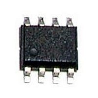
A25L040O-F AMIC, A25L040O-F Datasheet - Page 18

A25L040O-F
Manufacturer Part Number
A25L040O-F
Description
58T1309
Manufacturer
AMIC
Datasheet
1.A25L040-F.pdf
(39 pages)
Specifications of A25L040O-F
Memory Type
Flash
Memory Size
4Mbit
Memory Configuration
4M X 1
Interface Type
Serial, SPI
Clock Frequency
100MHz
Supply Voltage Range
2.7V To 3.6V
Memory Case Style
SOIC
No. Of Pins
8
Rohs Compliant
Yes
Available stocks
Company
Part Number
Manufacturer
Quantity
Price
Part Number:
A25L040O-F
Manufacturer:
AMIC
Quantity:
20 000
Page Program (PP)
The Page Program (PP) instruction allows bytes to be
programmed in the memory (changing bits from 1 to 0).
Before it can be accepted, a Write Enable (WREN) instruction
must previously have been executed. After the Write Enable
(WREN) instruction has been decoded, the device sets the
Write Enable Latch (WEL).
The Page Program (PP) instruction is entered by driving Chip
Select (
address bytes and at least one data byte on Serial Data Input
(DIO). If the 8 least significant address bits (A7-A0) are not all
zero, all transmitted data that goes beyond the end of the
current page are programmed from the start address of the
same page (from the address whose 8 least significant bits
(A7-A0) are all zero). Chip Select (
the entire duration of the sequence.
The instruction sequence is shown in Figure 12. If more than
256 bytes are sent to the device, previously latched data are
discarded and the last 256 data bytes are guaranteed to be
Figure 12. Page Program (PP) Instruction Sequence
(October, 2010, Version 1.2)
S
) Low, followed by the instruction code, three
DIO
DIO
S
S
C
C
Note: Address bits A23 to A19 are Don’t Care, for A25L040.
MSB
7 6 5 4 3 2 1
40
0 1
41
42
Data Byte 2
S
43
2 3 4
) must be driven Low for
Instruction
44
45
46
5 6
0
47
MSB
7 6 5 4 3 2 1 0
48
7
MSB
23 22 21
8
49
Data Byte 3
9
50
24-Bit Address
10
17
51
programmed correctly within the same page. If less than 256
Data bytes are sent to device, they are correctly programmed
at the requested addresses without having any effects on the
other bytes of the same page.
Chip Select (
last data byte has been latched in, otherwise the Page
Program (PP) instruction is not executed.
As soon as Chip Select (
Page Program cycle (whose duration is t
the Page Program cycle is in progress, the Status Register
may be read to check the value of the Write In Progress (WIP)
bit. The Write In Progress (WIP) bit is 1 during the self-timed
Page Program cycle, and is 0 when it is completed. At some
unspecified time before the cycle is completed, the Write
Enable Latch (WEL) bit is reset.
A Page Program (PP) instruction applied to a page which is
protected by the Block Protect (BP2, BP1, BP0) bits (see
Table 1. and Table 2.) is not executed.
52
3 2 1 0
3
28 29 30 31 32 33 34 35 36 37 38 39
53 54
55
S
) must be driven High after the eighth bit of the
MSB
7 6 5 4 3 2 1 0
MSB
7 6 5 4 3 2 1 0
Data Byte 256
Data Byte 1
AMIC Technology Corp.
S
) is driven High, the self-timed
A25L040 Series
PP
) is initiated. While


