C8051F020DK Silicon Laboratories Inc, C8051F020DK Datasheet - Page 141
C8051F020DK
Manufacturer Part Number
C8051F020DK
Description
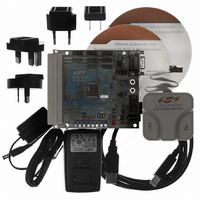
DEV KIT FOR F020/F021/F022/F023
Manufacturer
Silicon Laboratories Inc
Type
MCUr
Datasheet
1.C8051F020DK.pdf
(272 pages)
Specifications of C8051F020DK
Contents
Evaluation Board, Power Supply, USB Cables, Adapter and Documentation
Processor To Be Evaluated
C8051F02x
Interface Type
USB
Silicon Manufacturer
Silicon Labs
Core Architecture
8051
Silicon Core Number
C8051F020
Silicon Family Name
C8051F02x
Lead Free Status / RoHS Status
Contains lead / RoHS non-compliant
For Use With/related Products
Silicon Laboratories C8051 F020/021/022/023
Lead Free Status / Rohs Status
Lead free / RoHS Compliant
Other names
336-1200
Available stocks
Company
Part Number
Manufacturer
Quantity
Price
Company:

Part Number:
C8051F020DK
Manufacturer:
SiliconL
Quantity:
10


The lock bits can always be read and cleared to logic 0 regardless of the security setting applied to the block contain-
ing the security bytes. This allows additional blocks to be protected after the block containing the security bytes has
been locked. Important Note: The only means of removing a lock once set is to erase the entire program mem-
ory space by performing a JTAG erase operation (i.e. cannot be done in user firmware). Addressing either
security byte while performing a JTAG erase operation will automatically initiate erasure of the entire pro-
gram memory space (except for the reserved area). This erasure can only be performed via JTAG. If a non-
security byte in the 0xFBFF-0xFDFF page is addressed during the JTAG erasure, only that page (including the
security bytes) will be erased.
The FLASH Access Limit security feature (see Figure 15.1) protects proprietary program code and data from being
read by software running on the C8051F020/1/2/3. This feature provides support for OEMs that wish to program the
FLASH Read Lock Byte
Bits7-0: Each bit locks a corresponding block of memory. (Bit7 is MSB).
FLASH Write/Erase Lock Byte
Bits7-0: Each bit locks a corresponding block of memory.
FLASH access Limit Register (FLACL)
Read and Write/Erase Security Bits.
(Bit 7 is MSB.)
Bit
7
6
5
4
3
2
1
0
0xE000 - 0xFDFD
0xC000 - 0xDFFF
0xA000 - 0xBFFF
Memory Block
0x8000 - 0x9FFF
0x6000 - 0x7FFF
0x4000 - 0x5FFF
0x2000 - 0x3FFF
0x0000 - 0x1FFF
0: Read operations are locked (disabled) for corresponding block across the JTAG interface.
1: Read operations are unlocked (enabled) for corresponding block across the JTAG interface.
0: Write/Erase operations are locked (disabled) for corresponding block across the JTAG interface.
1: Write/Erase operations are unlocked (enabled) for corresponding block across the JTAG interface.
NOTE: When the highest block is locked, the security bytes may be written but not erased.
The content of this register is used as the high byte of the 16-bit software read limit address. This 16-
bit read limit address value is calculated as 0xNN00 where NN is replaced by content of this register
on reset. Software running at or above this address is prohibited from using the MOVX and MOVC
instructions to read, write, or erase FLASH locations below this address. Any attempts to read loca-
tions below this limit will return the value 0x00.
Figure 15.1. FLASH Program Memory Map and Security Bytes
Write/Erase Lock Byte
Software Read Limit
Read Lock Byte
SFLE = 0
Reserved
Rev. 1.4
0xFFFF
0xFE00
0xFDFF
0xFDFE
0xFDFD
0x0000
Memory Space
Program/Data
C8051F020/1/2/3
Scratchpad Memory
SFLE = 1
(Data only)
0x007F
0x0000
141
Related parts for C8051F020DK
Image
Part Number
Description
Manufacturer
Datasheet
Request
R

Part Number:
Description:
SMD/C°/SINGLE-ENDED OUTPUT SILICON OSCILLATOR
Manufacturer:
Silicon Laboratories Inc
Part Number:
Description:
Manufacturer:
Silicon Laboratories Inc
Datasheet:
Part Number:
Description:
N/A N/A/SI4010 AES KEYFOB DEMO WITH LCD RX
Manufacturer:
Silicon Laboratories Inc
Datasheet:
Part Number:
Description:
N/A N/A/SI4010 SIMPLIFIED KEY FOB DEMO WITH LED RX
Manufacturer:
Silicon Laboratories Inc
Datasheet:
Part Number:
Description:
N/A/-40 TO 85 OC/EZLINK MODULE; F930/4432 HIGH BAND (REV E/B1)
Manufacturer:
Silicon Laboratories Inc
Part Number:
Description:
EZLink Module; F930/4432 Low Band (rev e/B1)
Manufacturer:
Silicon Laboratories Inc
Part Number:
Description:
I°/4460 10 DBM RADIO TEST CARD 434 MHZ
Manufacturer:
Silicon Laboratories Inc
Part Number:
Description:
I°/4461 14 DBM RADIO TEST CARD 868 MHZ
Manufacturer:
Silicon Laboratories Inc
Part Number:
Description:
I°/4463 20 DBM RFSWITCH RADIO TEST CARD 460 MHZ
Manufacturer:
Silicon Laboratories Inc
Part Number:
Description:
I°/4463 20 DBM RADIO TEST CARD 868 MHZ
Manufacturer:
Silicon Laboratories Inc
Part Number:
Description:
I°/4463 27 DBM RADIO TEST CARD 868 MHZ
Manufacturer:
Silicon Laboratories Inc
Part Number:
Description:
I°/4463 SKYWORKS 30 DBM RADIO TEST CARD 915 MHZ
Manufacturer:
Silicon Laboratories Inc
Part Number:
Description:
N/A N/A/-40 TO 85 OC/4463 RFMD 30 DBM RADIO TEST CARD 915 MHZ
Manufacturer:
Silicon Laboratories Inc
Part Number:
Description:
I°/4463 20 DBM RADIO TEST CARD 169 MHZ
Manufacturer:
Silicon Laboratories Inc