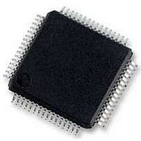
S9S12HY64J0MLH Freescale Semiconductor, S9S12HY64J0MLH Datasheet - Page 122

S9S12HY64J0MLH
Manufacturer Part Number
S9S12HY64J0MLH
Description
MCU 64K FLASH AUTO 64-LQFP
Manufacturer
Freescale Semiconductor
Series
HCS12r
Datasheet
1.S9S12HA32J0CLL.pdf
(792 pages)
Specifications of S9S12HY64J0MLH
Core Processor
HCS12
Core Size
16-Bit
Speed
32MHz
Connectivity
CAN, EBI/EMI, I²C, IrDA, LIN, SCI, SPI
Peripherals
LCD, Motor control PWM, POR, PWM, WDT
Number Of I /o
50
Program Memory Size
64KB (64K x 8)
Program Memory Type
FLASH
Eeprom Size
4K x 8
Ram Size
4K x 8
Voltage - Supply (vcc/vdd)
4.5 V ~ 5.5 V
Data Converters
A/D 6x10b
Oscillator Type
Internal
Operating Temperature
-40°C ~ 125°C
Package / Case
64-LQFP
Controller Family/series
S12
No. Of I/o's
50
Ram Memory Size
4KB
Cpu Speed
64MHz
No. Of Timers
2
Rohs Compliant
Yes
Processor Series
S12HY
Core
HCS12
3rd Party Development Tools
EWHCS12
Development Tools By Supplier
DEMO9S12HY64
Lead Free Status / RoHS Status
Lead free / RoHS Compliant
Available stocks
Company
Part Number
Manufacturer
Quantity
Price
Company:
Part Number:
S9S12HY64J0MLH
Manufacturer:
Freescale Semiconductor
Quantity:
10 000
- Current page: 122 of 792
- Download datasheet (4Mb)
1
Port Integration Module (S12HYPIMV1)
122
In order TIM1 input capture to be function correctly, need to disable all the output functions on the corresponding channel. Also
the corresponding SRRV bit should be set to 0.
Field
PTV
PTV
PTV
PTV
3
2
1
0
Port V general purpose input/output data—Data Register, Motor driver PWM output, SS of SPI, PWM channel 7,
SDA of IIC
Port V pin 3 is associated with the Motor PWM output, SPI and PWM channel 4 and IIC.
When not used with the alternative functions, this pin can be used as general purpose I/O. If the associated data
direction bit of this pins is set to 1, a read returns the value of the port register, otherwise the buffered pin input state
is read.
Port V general purpose input/output data—Data Register, Motor driver PWM output, TIM1 channel 1, SCK of SPI,
PWM channel 6
Port V pin 2 is associated with the Motor PWM output, SPI and PWM channel 7.
When not used with the alternative functions, this pin can be used as general purpose I/O. If the associated data
direction bit of this pins is set to 1, a read returns the value of the port register, otherwise the buffered pin input state
is read.
Port V general purpose input/output data—Data Register, Motor driver PWM output, MOSI of SPI, PWM channel
5
Port V pin 1 is associated with the Motor PWM output, SPI and PWM channel 6.
When not used with the alternative functions, this pin can be used as general purpose I/O. If the associated data
direction bit of this pins is set to 1, a read returns the value of the port register, otherwise the buffered pin input state
is read.
Port V general purpose input/output data—Data Register, Motor driver PWM output, TIM1 channel 0, MISO of
SPI, PWM channel 4, SCL of IIC
Port V pin 0 is associated with the Motor PWM output, TIM1 channel 0, SPI and PWM channel 5 and IIC.
When not used with the alternative functions, this pin can be used as general purpose I/O. If the associated data
direction bit of this pins is set to 1, a read returns the value of the port register, otherwise the buffered pin input state
is read.
• The Motor driver PWM takes precedence over the SPI, PWM channel 7, IIC and general purpose I/O function.
• The SDA of IIC takes precedence over the PWM channel 7, SPI and general purpose I/O function
• The PWM channel 7 takes precedence over the SPI and general purpose I/O function
• The SS of SPI takes precedence over the general purpose I/O function
• The Motor driver PWM takes precedence over the TIM1, SPI, PWM channel 6 and general purpose I/O function.
• The TIM1 channel 1 output function takes precedence over the SPI, PWM channels 6 and the general purpose
• The SCK of SPI takes precedence over the PWM channel 6 and the general purpose I/O function
• The PWM channel 6 takes precedence over the general purpose I/O function
• The Motor driver PWM takes precedence over the SPI, PWM channel 5 and general purpose I/O function.
• The MOSI of SPI takes precedence over the PWM channel 5 and the general purpose I/O function
• The PWM channel 5 takes precedence over the general purpose I/O function
• The Motor driver PWM takes precedence over the TIM1, SPI, PWM channel 4, IIC and general purpose I/O
• The TIM1 output compare function take precedence over the SPI, PWM channel4, IIC and general purpose I/O
• The SCL of IIC takes presentees over the PWM channel 4, SPI and general purpose I/O function
• The PWM channel 4 takes precedence over the SPI and the general purpose I/O function
• The MISO of SPI takes precedence over the general purpose I/O function
I/O function if related channel is enabled
function.
MC9S12HY/HA-Family Reference Manual, Rev. 1.04
Table 2-68. PTV register Field Descriptions
1
Description
Freescale Semiconductor
1
Related parts for S9S12HY64J0MLH
Image
Part Number
Description
Manufacturer
Datasheet
Request
R
Part Number:
Description:
Manufacturer:
Freescale Semiconductor, Inc
Datasheet:
Part Number:
Description:
Manufacturer:
Freescale Semiconductor, Inc
Datasheet:
Part Number:
Description:
Manufacturer:
Freescale Semiconductor, Inc
Datasheet:
Part Number:
Description:
Manufacturer:
Freescale Semiconductor, Inc
Datasheet:
Part Number:
Description:
Manufacturer:
Freescale Semiconductor, Inc
Datasheet:
Part Number:
Description:
Manufacturer:
Freescale Semiconductor, Inc
Datasheet:
Part Number:
Description:
Manufacturer:
Freescale Semiconductor, Inc
Datasheet:
Part Number:
Description:
Manufacturer:
Freescale Semiconductor, Inc
Datasheet:
Part Number:
Description:
Manufacturer:
Freescale Semiconductor, Inc
Datasheet:
Part Number:
Description:
Manufacturer:
Freescale Semiconductor, Inc
Datasheet:
Part Number:
Description:
Manufacturer:
Freescale Semiconductor, Inc
Datasheet:
Part Number:
Description:
Manufacturer:
Freescale Semiconductor, Inc
Datasheet:
Part Number:
Description:
Manufacturer:
Freescale Semiconductor, Inc
Datasheet:
Part Number:
Description:
Manufacturer:
Freescale Semiconductor, Inc
Datasheet:
Part Number:
Description:
Manufacturer:
Freescale Semiconductor, Inc
Datasheet:


