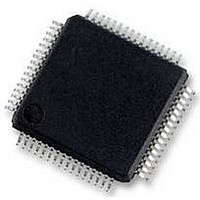
S9S12HY64J0MLH Freescale Semiconductor, S9S12HY64J0MLH Datasheet - Page 497

S9S12HY64J0MLH
Manufacturer Part Number
S9S12HY64J0MLH
Description
MCU 64K FLASH AUTO 64-LQFP
Manufacturer
Freescale Semiconductor
Series
HCS12r
Datasheet
1.S9S12HA32J0CLL.pdf
(792 pages)
Specifications of S9S12HY64J0MLH
Core Processor
HCS12
Core Size
16-Bit
Speed
32MHz
Connectivity
CAN, EBI/EMI, I²C, IrDA, LIN, SCI, SPI
Peripherals
LCD, Motor control PWM, POR, PWM, WDT
Number Of I /o
50
Program Memory Size
64KB (64K x 8)
Program Memory Type
FLASH
Eeprom Size
4K x 8
Ram Size
4K x 8
Voltage - Supply (vcc/vdd)
4.5 V ~ 5.5 V
Data Converters
A/D 6x10b
Oscillator Type
Internal
Operating Temperature
-40°C ~ 125°C
Package / Case
64-LQFP
Controller Family/series
S12
No. Of I/o's
50
Ram Memory Size
4KB
Cpu Speed
64MHz
No. Of Timers
2
Rohs Compliant
Yes
Processor Series
S12HY
Core
HCS12
3rd Party Development Tools
EWHCS12
Development Tools By Supplier
DEMO9S12HY64
Lead Free Status / RoHS Status
Lead free / RoHS Compliant
Available stocks
Company
Part Number
Manufacturer
Quantity
Price
Company:
Part Number:
S9S12HY64J0MLH
Manufacturer:
Freescale Semiconductor
Quantity:
10 000
- Current page: 497 of 792
- Download datasheet (4Mb)
14.3.2.8
Read: Anytime
Write: Anytime
Freescale Semiconductor
Module Base + 0x0008
Module Base + 0x0009
Reset
Reset
Field
OMx
OLx
7:0
7:0
W
W
R
R
OM7
OM3
Output Mode — These eight pairs of control bits are encoded to specify the output action to be taken as a result
of a successful OCx compare. When either OMx or OLx is 1, the pin associated with OCx becomes an output
tied to OCx.
Note: To enable output action by OMx bits on timer port, the corresponding bit in OC7M should be cleared. For
Output Level — These eight pairs of control bits are encoded to specify the output action to be taken as a result
of a successful OCx compare. When either OMx or OLx is 1, the pin associated with OCx becomes an output
tied to OCx.
Note: To enable output action by OLx bits on timer port, the corresponding bit in OC7M should be cleared. For
Timer Control Register 1/Timer Control Register 2 (TCTL1/TCTL2)
0
0
7
7
an output line to be driven by an OCx the OCPDx must be cleared.
an output line to be driven by an OCx the OCPDx must be cleared.
OMx
OL7
OL3
0
0
6
6
0
0
1
1
Figure 14-14. Timer Control Register 1 (TCTL1)
Figure 14-15. Timer Control Register 2 (TCTL2)
MC9S12HY/HA-Family Reference Manual Rev. 1.04
Table 14-8. TCTL1/TCTL2 Field Descriptions
Table 14-9. Compare Result Output Action
OM6
OM2
OLx
0
1
0
1
0
0
5
5
OL6
OL2
0
0
4
4
action on the timer output signal
Clear OCx output line to zero
Description
Set OCx output line to one
Toggle OCx output line
No output compare
OM5
OM1
Action
0
0
3
3
Timer Module (TIM16B8CV2) Block Description
OL5
OL1
0
0
2
2
OM4
OM0
0
0
1
1
OL4
OL0
0
0
0
0
497
Related parts for S9S12HY64J0MLH
Image
Part Number
Description
Manufacturer
Datasheet
Request
R
Part Number:
Description:
Manufacturer:
Freescale Semiconductor, Inc
Datasheet:
Part Number:
Description:
Manufacturer:
Freescale Semiconductor, Inc
Datasheet:
Part Number:
Description:
Manufacturer:
Freescale Semiconductor, Inc
Datasheet:
Part Number:
Description:
Manufacturer:
Freescale Semiconductor, Inc
Datasheet:
Part Number:
Description:
Manufacturer:
Freescale Semiconductor, Inc
Datasheet:
Part Number:
Description:
Manufacturer:
Freescale Semiconductor, Inc
Datasheet:
Part Number:
Description:
Manufacturer:
Freescale Semiconductor, Inc
Datasheet:
Part Number:
Description:
Manufacturer:
Freescale Semiconductor, Inc
Datasheet:
Part Number:
Description:
Manufacturer:
Freescale Semiconductor, Inc
Datasheet:
Part Number:
Description:
Manufacturer:
Freescale Semiconductor, Inc
Datasheet:
Part Number:
Description:
Manufacturer:
Freescale Semiconductor, Inc
Datasheet:
Part Number:
Description:
Manufacturer:
Freescale Semiconductor, Inc
Datasheet:
Part Number:
Description:
Manufacturer:
Freescale Semiconductor, Inc
Datasheet:
Part Number:
Description:
Manufacturer:
Freescale Semiconductor, Inc
Datasheet:
Part Number:
Description:
Manufacturer:
Freescale Semiconductor, Inc
Datasheet:


