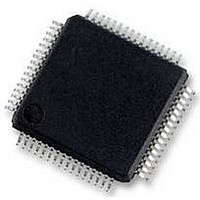
S9S12HY64J0MLH Freescale Semiconductor, S9S12HY64J0MLH Datasheet - Page 44

S9S12HY64J0MLH
Manufacturer Part Number
S9S12HY64J0MLH
Description
MCU 64K FLASH AUTO 64-LQFP
Manufacturer
Freescale Semiconductor
Series
HCS12r
Datasheet
1.S9S12HA32J0CLL.pdf
(792 pages)
Specifications of S9S12HY64J0MLH
Core Processor
HCS12
Core Size
16-Bit
Speed
32MHz
Connectivity
CAN, EBI/EMI, I²C, IrDA, LIN, SCI, SPI
Peripherals
LCD, Motor control PWM, POR, PWM, WDT
Number Of I /o
50
Program Memory Size
64KB (64K x 8)
Program Memory Type
FLASH
Eeprom Size
4K x 8
Ram Size
4K x 8
Voltage - Supply (vcc/vdd)
4.5 V ~ 5.5 V
Data Converters
A/D 6x10b
Oscillator Type
Internal
Operating Temperature
-40°C ~ 125°C
Package / Case
64-LQFP
Controller Family/series
S12
No. Of I/o's
50
Ram Memory Size
4KB
Cpu Speed
64MHz
No. Of Timers
2
Rohs Compliant
Yes
Processor Series
S12HY
Core
HCS12
3rd Party Development Tools
EWHCS12
Development Tools By Supplier
DEMO9S12HY64
Lead Free Status / RoHS Status
Lead free / RoHS Compliant
Available stocks
Company
Part Number
Manufacturer
Quantity
Price
Company:
Part Number:
S9S12HY64J0MLH
Manufacturer:
Freescale Semiconductor
Quantity:
10 000
- Current page: 44 of 792
- Download datasheet (4Mb)
Device Overview MC9S12HY/HA-Family
(during master mode) or slave input pin (during slave mode) MOSI of the serial peripheral interface (SPI).
It can be configured as PWM channel 5.
1.7.3.49
PV0 is a general-purpose input or output pin. It can be configured as high current PWM output pin which
can be used for motor driver. It interface to the coil of motor 2. It can be configured as timer (TIM1)
channel 0. It can be configured as the master input (during master mode) or slave output pin (during slave
mode) MISO for the serial peripheral interface (SPI). It can be configured as the serial clock pin SCL of
IIC module. It can be configured as PWM channel 4.
1.7.4
MC9S12HY/HA-Family power and ground pins are described below. Because fast signal transitions place
high, short-duration current demands on the power supply, use bypass capacitors with high-frequency
characteristics and place them as close to the MCU as possible.
1.7.4.1
External power and ground for I/O drivers. Bypass requirements depend on how heavily the MCU pins are
loaded.
1.7.4.2
Power supply input to the internal voltage regulator.
1.7.4.3
The voltage supply of nominally 1.8 V is derived from the internal voltage regulator. The return current
path is through the VSS3 pin. No static external loading of these pins is permitted.
1.7.4.4
This pin provides ground for the oscillator and the phased-locked loop. The voltage supply of nominally
1.8 V is derived from the internal voltage regulator. On 64LQFP, it will be bonded together with VSS3.
1.7.4.5
These are the power supply and ground input pins for Port AD IO, the analog-to-digital converter and the
voltage regulator. And also server as the reference voltage input pins for the analog-to-digital converter.
44
Power Supply Pins
PV0 / MISO / PWM4 / SCL / IOC1_0 / M2C0M — Port V I/O Pin 0
VDDX / VSSX — Power and Ground Pins for I/O Drivers
VDDR — Power Pin for Internal Voltage Regulator
VSS3 — Core Ground Pin
VSSPLL — Ground Pin for PLL
VDDA/VRH / VSSA/VRL — Power Supply Pins for ATD and Voltage
Regulator and ATD Reference Voltage inputs
All V
SS
pins must be connected together in the application.
MC9S12HY/HA-Family Reference Manual, Rev. 1.04
NOTE
Freescale Semiconductor
Related parts for S9S12HY64J0MLH
Image
Part Number
Description
Manufacturer
Datasheet
Request
R
Part Number:
Description:
Manufacturer:
Freescale Semiconductor, Inc
Datasheet:
Part Number:
Description:
Manufacturer:
Freescale Semiconductor, Inc
Datasheet:
Part Number:
Description:
Manufacturer:
Freescale Semiconductor, Inc
Datasheet:
Part Number:
Description:
Manufacturer:
Freescale Semiconductor, Inc
Datasheet:
Part Number:
Description:
Manufacturer:
Freescale Semiconductor, Inc
Datasheet:
Part Number:
Description:
Manufacturer:
Freescale Semiconductor, Inc
Datasheet:
Part Number:
Description:
Manufacturer:
Freescale Semiconductor, Inc
Datasheet:
Part Number:
Description:
Manufacturer:
Freescale Semiconductor, Inc
Datasheet:
Part Number:
Description:
Manufacturer:
Freescale Semiconductor, Inc
Datasheet:
Part Number:
Description:
Manufacturer:
Freescale Semiconductor, Inc
Datasheet:
Part Number:
Description:
Manufacturer:
Freescale Semiconductor, Inc
Datasheet:
Part Number:
Description:
Manufacturer:
Freescale Semiconductor, Inc
Datasheet:
Part Number:
Description:
Manufacturer:
Freescale Semiconductor, Inc
Datasheet:
Part Number:
Description:
Manufacturer:
Freescale Semiconductor, Inc
Datasheet:
Part Number:
Description:
Manufacturer:
Freescale Semiconductor, Inc
Datasheet:


