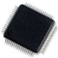
S9S12HY64J0MLH Freescale Semiconductor, S9S12HY64J0MLH Datasheet - Page 673

S9S12HY64J0MLH
Manufacturer Part Number
S9S12HY64J0MLH
Description
MCU 64K FLASH AUTO 64-LQFP
Manufacturer
Freescale Semiconductor
Series
HCS12r
Datasheet
1.S9S12HA32J0CLL.pdf
(792 pages)
Specifications of S9S12HY64J0MLH
Core Processor
HCS12
Core Size
16-Bit
Speed
32MHz
Connectivity
CAN, EBI/EMI, I²C, IrDA, LIN, SCI, SPI
Peripherals
LCD, Motor control PWM, POR, PWM, WDT
Number Of I /o
50
Program Memory Size
64KB (64K x 8)
Program Memory Type
FLASH
Eeprom Size
4K x 8
Ram Size
4K x 8
Voltage - Supply (vcc/vdd)
4.5 V ~ 5.5 V
Data Converters
A/D 6x10b
Oscillator Type
Internal
Operating Temperature
-40°C ~ 125°C
Package / Case
64-LQFP
Controller Family/series
S12
No. Of I/o's
50
Ram Memory Size
4KB
Cpu Speed
64MHz
No. Of Timers
2
Rohs Compliant
Yes
Processor Series
S12HY
Core
HCS12
3rd Party Development Tools
EWHCS12
Development Tools By Supplier
DEMO9S12HY64
Lead Free Status / RoHS Status
Lead free / RoHS Compliant
Available stocks
Company
Part Number
Manufacturer
Quantity
Price
Company:
Part Number:
S9S12HY64J0MLH
Manufacturer:
Freescale Semiconductor
Quantity:
10 000
- Current page: 673 of 792
- Download datasheet (4Mb)
18.4
This section provides a complete functional description of the LCD40F4BV1 block, detailing the
operation of the design from the end user perspective in a number of subsections.
18.4.1
18.4.1.1
During a reset the following conditions exist:
18.4.1.2
The frequency of the source clock (IRCCLK) and divider determine the LCD clock frequency. The divider
is set by the LCD clock prescaler bits, LCLK[2:0], in the LCD control register 0 (LCDCR0).
shows the LCD clock and frame frequency for some multiplexed mode at IRCCLK = 16 MHz, 8 MHz, 4
MHz, 2 MHz, 1 MHz, and 0.5 MHz.
Freescale Semiconductor
Source clock
Frequency in
IRCCLK = 0.5
IRCCLK = 1.0
IRCCLK = 2.0
IRCCLK = 4.0
IRCCLK = 8.0
FP[39:0]
BP[3:0]
Field
•
•
39:0
3:0
MHz
The LCD40F4BV1 system is configured in the default mode, 1/4 duty and 1/3 bias, that means all
backplanes are used.
All frontplane enable bits, FP[39:0]EN are cleared and the ON/OFF control for the display, the
LCDEN bit is cleared, thereby forcing all frontplane and backplane driver outputs to the high
impedance state. The MCU pin state during reset is defined by the port integration module (PIM).
Functional Description
LCD Driver Description
LCD Segment ON — The FP[39:0]BP[3:0] bit displays (turns on) the LCD segment connected between FP[39:0]
and BP[3:0].
0 LCD segment OFF
1 LCD segment ON
Frontplane, Backplane, and LCD System During Reset
LCD Clock and Frame Frequency
LCLK2
LCD Clock Prescaler
0
0
0
0
0
0
0
1
1
1
LCLK1
0
0
0
1
1
1
1
0
0
0
MC9S12HY/HA-Family Reference Manual, Rev. 1.04
Table 18-8. LCD Clock and Frame Frequency
Table 18-7. LCD RAM Field Descriptions
LCLK0
0
1
1
0
0
1
1
0
0
1
Divider
16384
16384
32768
1024
2048
2048
4096
4096
8192
8192
Frequency [Hz]
Description
LCD Clock
488
244
488
244
488
244
488
244
488
244
Liquid Crystal Display (LCD40F4BV1) Block Description
1/1 Duty
488
244
488
244
488
244
488
244
488
244
Frame Frequency [Hz]
1/2 Duty
244
122
244
122
244
122
244
122
244
122
1/3 Duty
163
163
163
163
163
81
81
81
81
81
Table 18-8
1/4 Duty
122
122
122
122
122
61
61
61
61
61
673
Related parts for S9S12HY64J0MLH
Image
Part Number
Description
Manufacturer
Datasheet
Request
R
Part Number:
Description:
Manufacturer:
Freescale Semiconductor, Inc
Datasheet:
Part Number:
Description:
Manufacturer:
Freescale Semiconductor, Inc
Datasheet:
Part Number:
Description:
Manufacturer:
Freescale Semiconductor, Inc
Datasheet:
Part Number:
Description:
Manufacturer:
Freescale Semiconductor, Inc
Datasheet:
Part Number:
Description:
Manufacturer:
Freescale Semiconductor, Inc
Datasheet:
Part Number:
Description:
Manufacturer:
Freescale Semiconductor, Inc
Datasheet:
Part Number:
Description:
Manufacturer:
Freescale Semiconductor, Inc
Datasheet:
Part Number:
Description:
Manufacturer:
Freescale Semiconductor, Inc
Datasheet:
Part Number:
Description:
Manufacturer:
Freescale Semiconductor, Inc
Datasheet:
Part Number:
Description:
Manufacturer:
Freescale Semiconductor, Inc
Datasheet:
Part Number:
Description:
Manufacturer:
Freescale Semiconductor, Inc
Datasheet:
Part Number:
Description:
Manufacturer:
Freescale Semiconductor, Inc
Datasheet:
Part Number:
Description:
Manufacturer:
Freescale Semiconductor, Inc
Datasheet:
Part Number:
Description:
Manufacturer:
Freescale Semiconductor, Inc
Datasheet:
Part Number:
Description:
Manufacturer:
Freescale Semiconductor, Inc
Datasheet:


