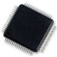
S9S12HY64J0MLH Freescale Semiconductor, S9S12HY64J0MLH Datasheet - Page 17

S9S12HY64J0MLH
Manufacturer Part Number
S9S12HY64J0MLH
Description
MCU 64K FLASH AUTO 64-LQFP
Manufacturer
Freescale Semiconductor
Series
HCS12r
Datasheet
1.S9S12HA32J0CLL.pdf
(792 pages)
Specifications of S9S12HY64J0MLH
Core Processor
HCS12
Core Size
16-Bit
Speed
32MHz
Connectivity
CAN, EBI/EMI, I²C, IrDA, LIN, SCI, SPI
Peripherals
LCD, Motor control PWM, POR, PWM, WDT
Number Of I /o
50
Program Memory Size
64KB (64K x 8)
Program Memory Type
FLASH
Eeprom Size
4K x 8
Ram Size
4K x 8
Voltage - Supply (vcc/vdd)
4.5 V ~ 5.5 V
Data Converters
A/D 6x10b
Oscillator Type
Internal
Operating Temperature
-40°C ~ 125°C
Package / Case
64-LQFP
Controller Family/series
S12
No. Of I/o's
50
Ram Memory Size
4KB
Cpu Speed
64MHz
No. Of Timers
2
Rohs Compliant
Yes
Processor Series
S12HY
Core
HCS12
3rd Party Development Tools
EWHCS12
Development Tools By Supplier
DEMO9S12HY64
Lead Free Status / RoHS Status
Lead free / RoHS Compliant
Available stocks
Company
Part Number
Manufacturer
Quantity
Price
Company:
Part Number:
S9S12HY64J0MLH
Manufacturer:
Freescale Semiconductor
Quantity:
10 000
- Current page: 17 of 792
- Download datasheet (4Mb)
1.3.15
1.3.16
1.3.17
Freescale Semiconductor
•
•
•
•
•
•
•
•
•
•
•
•
•
•
•
•
•
•
•
•
•
— 8 x 8-bit
Wakeup with integrated low pass filter option
Loop back for self test
Listen-only mode to monitor CAN bus
Bus-off recovery by software intervention or automatically
16-bit time stamp of transmitted/received messages
Full-duplex or single-wire operation
Standard mark/space non-return-to-zero (NRZ) format
Selectable IrDA 1.4 return-to-zero-inverted (RZI) format with programmable pulse widths
13-bit baud rate selection
Programmable character length
Programmable polarity for transmitter and receiver
Active edge receive wakeup
Break detect and transmit collision detect supporting LIN
Configurable 8- or 16-bit data size
Full-duplex or single-wire bidirectional
Double-buffered transmit and receive
Master or slave mode
MSB-first or LSB-first shifting
Serial clock phase and polarity options
Up to 8-channel, 10-bit analog-to-digital converter
— 3 s single conversion time
— 8-/10 bit resolution
— Left or right justified result data
— Internal oscillator for conversion in stop modes
— Wakeup from low power modes on analog comparison > or <= match
— Continuous conversion mode
— Multiple channel scans
Pins can also be used as digital I/O
Serial Communication Interface Module (SCI)
Serial Peripheral Interface Module (SPI)
Analog-to-Digital Converter Module (ATD)
MC9S12HY/HA-Family Reference Manual, Rev. 1.04
Device Overview MC9S12HY/HA-Family
17
Related parts for S9S12HY64J0MLH
Image
Part Number
Description
Manufacturer
Datasheet
Request
R
Part Number:
Description:
Manufacturer:
Freescale Semiconductor, Inc
Datasheet:
Part Number:
Description:
Manufacturer:
Freescale Semiconductor, Inc
Datasheet:
Part Number:
Description:
Manufacturer:
Freescale Semiconductor, Inc
Datasheet:
Part Number:
Description:
Manufacturer:
Freescale Semiconductor, Inc
Datasheet:
Part Number:
Description:
Manufacturer:
Freescale Semiconductor, Inc
Datasheet:
Part Number:
Description:
Manufacturer:
Freescale Semiconductor, Inc
Datasheet:
Part Number:
Description:
Manufacturer:
Freescale Semiconductor, Inc
Datasheet:
Part Number:
Description:
Manufacturer:
Freescale Semiconductor, Inc
Datasheet:
Part Number:
Description:
Manufacturer:
Freescale Semiconductor, Inc
Datasheet:
Part Number:
Description:
Manufacturer:
Freescale Semiconductor, Inc
Datasheet:
Part Number:
Description:
Manufacturer:
Freescale Semiconductor, Inc
Datasheet:
Part Number:
Description:
Manufacturer:
Freescale Semiconductor, Inc
Datasheet:
Part Number:
Description:
Manufacturer:
Freescale Semiconductor, Inc
Datasheet:
Part Number:
Description:
Manufacturer:
Freescale Semiconductor, Inc
Datasheet:
Part Number:
Description:
Manufacturer:
Freescale Semiconductor, Inc
Datasheet:


