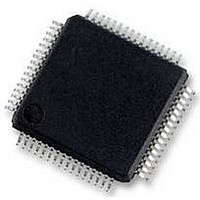
S9S12HY64J0MLH Freescale Semiconductor, S9S12HY64J0MLH Datasheet - Page 668

S9S12HY64J0MLH
Manufacturer Part Number
S9S12HY64J0MLH
Description
MCU 64K FLASH AUTO 64-LQFP
Manufacturer
Freescale Semiconductor
Series
HCS12r
Datasheet
1.S9S12HA32J0CLL.pdf
(792 pages)
Specifications of S9S12HY64J0MLH
Core Processor
HCS12
Core Size
16-Bit
Speed
32MHz
Connectivity
CAN, EBI/EMI, I²C, IrDA, LIN, SCI, SPI
Peripherals
LCD, Motor control PWM, POR, PWM, WDT
Number Of I /o
50
Program Memory Size
64KB (64K x 8)
Program Memory Type
FLASH
Eeprom Size
4K x 8
Ram Size
4K x 8
Voltage - Supply (vcc/vdd)
4.5 V ~ 5.5 V
Data Converters
A/D 6x10b
Oscillator Type
Internal
Operating Temperature
-40°C ~ 125°C
Package / Case
64-LQFP
Controller Family/series
S12
No. Of I/o's
50
Ram Memory Size
4KB
Cpu Speed
64MHz
No. Of Timers
2
Rohs Compliant
Yes
Processor Series
S12HY
Core
HCS12
3rd Party Development Tools
EWHCS12
Development Tools By Supplier
DEMO9S12HY64
Lead Free Status / RoHS Status
Lead free / RoHS Compliant
Available stocks
Company
Part Number
Manufacturer
Quantity
Price
Company:
Part Number:
S9S12HY64J0MLH
Manufacturer:
Freescale Semiconductor
Quantity:
10 000
- Current page: 668 of 792
- Download datasheet (4Mb)
Liquid Crystal Display (LCD40F4BV1) Block Description
18.3.2
This section consists of register descriptions. Each description includes a standard register diagram.
Details of register bit and field function follow the register diagrams, in bit order.
18.3.2.1
Read: anytime
Write: LCDEN anytime. To avoid segment flicker the clock prescaler bits, the bias select bit and the duty
668
Module Base + 0x0000
DUTY[1:0]
LCLK[2:0]
LCDEN
Reset
Field
BIAS
5:3
1:0
7
2
W
R
select bits must not be changed when the LCD is enabled.
LCDEN
Register Descriptions
LCD40F4BV1 Driver System Enable — The LCDEN bit starts the LCD waveform generator.
0 All frontplane and backplane pins are disabled. In addition, the LCD40F4BV1 system is disabled
1 LCD driver system is enabled. All FP[39:0] pins with FP[39:0]EN set, will output an LCD driver
LCD Clock Prescaler — The LCD clock prescaler bits determine the IRCCLK divider value to produce the LCD
clock frequency. For detailed description of the correlation between LCD clock prescaler bits and the divider
value please refer to
BIAS Voltage Level Select — This bit selects the bias voltage levels during various LCD operating modes, as
shown in
LCD Duty Select — The DUTY1 and DUTY0 bits select the duty (multiplex mode) of the LCD40F4BV1 driver
system, as shown in
LCD Control Register 0 (LCDCR0)
7
0
and all LCD waveform generation clocks are stopped.
waveform The BP[3:0] pins will output an LCD40F4BV1 driver waveform based on the settings of DUTY0
and DUTY1.
Table
= Unimplemented or Reserved
18-9.
6
0
0
Figure 18-2. LCD Control Register 0 (LCDCR0)
MC9S12HY/HA-Family Reference Manual, Rev. 1.04
Table
Table
Table 18-4. LCDCR0 Field Descriptions
18-8.
18-9.
LCLK2
5
0
LCLK1
4
0
Description
LCLK0
3
0
BIAS
2
0
DUTY1
Freescale Semiconductor
1
0
DUTY0
0
0
Related parts for S9S12HY64J0MLH
Image
Part Number
Description
Manufacturer
Datasheet
Request
R
Part Number:
Description:
Manufacturer:
Freescale Semiconductor, Inc
Datasheet:
Part Number:
Description:
Manufacturer:
Freescale Semiconductor, Inc
Datasheet:
Part Number:
Description:
Manufacturer:
Freescale Semiconductor, Inc
Datasheet:
Part Number:
Description:
Manufacturer:
Freescale Semiconductor, Inc
Datasheet:
Part Number:
Description:
Manufacturer:
Freescale Semiconductor, Inc
Datasheet:
Part Number:
Description:
Manufacturer:
Freescale Semiconductor, Inc
Datasheet:
Part Number:
Description:
Manufacturer:
Freescale Semiconductor, Inc
Datasheet:
Part Number:
Description:
Manufacturer:
Freescale Semiconductor, Inc
Datasheet:
Part Number:
Description:
Manufacturer:
Freescale Semiconductor, Inc
Datasheet:
Part Number:
Description:
Manufacturer:
Freescale Semiconductor, Inc
Datasheet:
Part Number:
Description:
Manufacturer:
Freescale Semiconductor, Inc
Datasheet:
Part Number:
Description:
Manufacturer:
Freescale Semiconductor, Inc
Datasheet:
Part Number:
Description:
Manufacturer:
Freescale Semiconductor, Inc
Datasheet:
Part Number:
Description:
Manufacturer:
Freescale Semiconductor, Inc
Datasheet:
Part Number:
Description:
Manufacturer:
Freescale Semiconductor, Inc
Datasheet:


