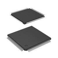
D12363VTE33 Renesas Electronics America, D12363VTE33 Datasheet - Page 43

D12363VTE33
Manufacturer Part Number
D12363VTE33
Description
MCU 3V 0K 120-TQFP
Manufacturer
Renesas Electronics America
Series
H8® H8S/2300r
Datasheet
1.DF2368VTE34V.pdf
(1044 pages)
Specifications of D12363VTE33
Core Processor
H8S/2000
Core Size
16-Bit
Speed
33MHz
Connectivity
I²C, IrDA, SCI, SmartCard
Peripherals
DMA, POR, PWM, WDT
Number Of I /o
84
Program Memory Type
ROMless
Ram Size
16K x 8
Voltage - Supply (vcc/vdd)
3 V ~ 3.6 V
Data Converters
A/D 10x10b, D/A 2x8b
Oscillator Type
Internal
Operating Temperature
-20°C ~ 75°C
Package / Case
120-TQFP, 120-VQFP
Lead Free Status / RoHS Status
Contains lead / RoHS non-compliant
Eeprom Size
-
Program Memory Size
-
Other names
HD6412363VTE33
HD6412363VTE33
HD6412363VTE33
Available stocks
Company
Part Number
Manufacturer
Quantity
Price
Company:
Part Number:
D12363VTE33V
Manufacturer:
Renesas Electronics America
Quantity:
10 000
- Current page: 43 of 1044
- Download datasheet (6Mb)
Figure 6.19 Example of Timing when Chip Select Assertion Period is Extended .................... 164
Figure 6.20 DRAM Basic Access Timing (RAST = 0, CAST = 0)........................................... 168
Figure 6.21 Example of Access Timing with 3-State Column Address Output Cycle
Figure 6.22 Example of Access Timing when RAS Signal Goes Low from Beginning
Figure 6.23 Example of Timing with One Row Address Output Maintenance State
Figure 6.24 Example of Timing with Two-State Precharge Cycle (RAST = 0, CAST = 0)...... 172
Figure 6.25 Example of Wait State Insertion Timing (2-State Column Address Output) ........ 174
Figure 6.26 Example of Wait State Insertion Timing (3-State Column Address Output) ......... 175
Figure 6.27 2-CAS Control Timing (Upper Byte Write Access: RAST = 0, CAST = 0)......... 176
Figure 6.28 Example of 2-CAS DRAM Connection ................................................................. 177
Figure 6.29 Operation Timing in Fast Page Mode (RAST = 0, CAST = 0) .............................. 178
Figure 6.30 Operation Timing in Fast Page Mode (RAST = 0, CAST = 1) .............................. 179
Figure 6.31 Example of Operation Timing in RAS Down Mode (RAST = 0, CAST = 0)........ 180
Figure 6.32 Example of Operation Timing in RAS Up Mode (RAST = 0, CAST = 0)............. 181
Figure 6.33 RTCNT Operation.................................................................................................. 182
Figure 6.34 Compare Match Timing ......................................................................................... 183
Figure 6.35 CBR Refresh Timing.............................................................................................. 183
Figure 6.36 CBR Refresh Timing (RCW1 = 0, RCW0 = 1, RLW1 = 0, RLW0 = 0)................ 184
Figure 6.37 Example of CBR Refresh Timing (CBRM = 1) ..................................................... 185
Figure 6.38 Self-Refresh Timing ............................................................................................... 186
Figure 6.39 Example of Timing when Precharge Time after Self-Refreshing Is Extended
Figure 6.40 Example of DACK Output Timing when DDS = 1 (RAST = 0, CAST = 0) ......... 188
Figure 6.41 Example of DACK Output Timing when DDS = 0 (RAST = 0, CAST = 1) ......... 189
Figure 6.42 Example of Burst ROM Access Timing (ASTn = 1, 2-State Burst Cycle) ............ 191
Figure 6.43 Example of Burst ROM Access Timing (ASTn = 0, 1-State Burst Cycle) ............ 192
Figure 6.44 xample of Idle Cycle Operation (Consecutive Reads in Different Areas).............. 193
Figure 6.45 Example of Idle Cycle Operation (Write after Read) ............................................. 194
Figure 6.46 Example of Idle Cycle Operation (Read after Write) ............................................. 195
Figure 6.47 Relationship between Chip Select (CS) and Read (RD)......................................... 196
Figure 6.48 Example of DRAM Full Access after External Read (CAST = 0) ......................... 196
Figure 6.49 Example of Idle Cycle Operation in RAS Down Mode (Consecutive Reads
Figure 6.50 Example of Idle Cycle Operation in RAS Down Mode (Write after Read)
Figure 6.51 Example of Idle Cycle Operation after DRAM Access (Consecutive Reads in
(RAST = 0)............................................................................................................. 169
of T
(RAST = 0, CAST = 0) .......................................................................................... 171
by 2 States .............................................................................................................. 187
in Different Areas) (IDLC = 0, RAST = 0, CAST = 0).......................................... 197
(IDLC = 0, RAST = 0, CAST = 0) ......................................................................... 198
Different Areas) (IDLC = 0, RAST = 0, CAST = 0).............................................. 199
r
State (CAST = 0) ........................................................................................... 170
Rev.6.00 Mar. 18, 2009 Page xli of lviii
REJ09B0050-0600
Related parts for D12363VTE33
Image
Part Number
Description
Manufacturer
Datasheet
Request
R

Part Number:
Description:
KIT STARTER FOR M16C/29
Manufacturer:
Renesas Electronics America
Datasheet:

Part Number:
Description:
KIT STARTER FOR R8C/2D
Manufacturer:
Renesas Electronics America
Datasheet:

Part Number:
Description:
R0K33062P STARTER KIT
Manufacturer:
Renesas Electronics America
Datasheet:

Part Number:
Description:
KIT STARTER FOR R8C/23 E8A
Manufacturer:
Renesas Electronics America
Datasheet:

Part Number:
Description:
KIT STARTER FOR R8C/25
Manufacturer:
Renesas Electronics America
Datasheet:

Part Number:
Description:
KIT STARTER H8S2456 SHARPE DSPLY
Manufacturer:
Renesas Electronics America
Datasheet:

Part Number:
Description:
KIT STARTER FOR R8C38C
Manufacturer:
Renesas Electronics America
Datasheet:

Part Number:
Description:
KIT STARTER FOR R8C35C
Manufacturer:
Renesas Electronics America
Datasheet:

Part Number:
Description:
KIT STARTER FOR R8CL3AC+LCD APPS
Manufacturer:
Renesas Electronics America
Datasheet:

Part Number:
Description:
KIT STARTER FOR RX610
Manufacturer:
Renesas Electronics America
Datasheet:

Part Number:
Description:
KIT STARTER FOR R32C/118
Manufacturer:
Renesas Electronics America
Datasheet:

Part Number:
Description:
KIT DEV RSK-R8C/26-29
Manufacturer:
Renesas Electronics America
Datasheet:

Part Number:
Description:
KIT STARTER FOR SH7124
Manufacturer:
Renesas Electronics America
Datasheet:

Part Number:
Description:
KIT STARTER FOR H8SX/1622
Manufacturer:
Renesas Electronics America
Datasheet:

Part Number:
Description:
KIT DEV FOR SH7203
Manufacturer:
Renesas Electronics America
Datasheet:


