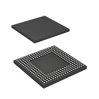
D17760BP200ADV Renesas Electronics America, D17760BP200ADV Datasheet - Page 157

D17760BP200ADV
Manufacturer Part Number
D17760BP200ADV
Description
MPU 3V 8K,PB-FREE, 256-BGA
Manufacturer
Renesas Electronics America
Series
SuperH® SH7750r
Datasheet
1.D6417760BP200ADV.pdf
(1418 pages)
Specifications of D17760BP200ADV
Core Processor
SH-4
Core Size
32-Bit
Speed
200MHz
Connectivity
Audio Codec, CAN, EBI/EMI, FIFO, I²C, MFI, MMC, SCI, Serial Sound, SIM, SPI, USB
Peripherals
DMA, LCD, POR, WDT
Number Of I /o
69
Program Memory Type
ROMless
Ram Size
48K x 8
Voltage - Supply (vcc/vdd)
1.4 V ~ 1.6 V
Data Converters
A/D 4x10b
Oscillator Type
Internal
Operating Temperature
-40°C ~ 85°C
Package / Case
256-BGA
Lead Free Status / RoHS Status
Lead free / RoHS Compliant
Eeprom Size
-
Program Memory Size
-
Available stocks
Company
Part Number
Manufacturer
Quantity
Price
Company:
Part Number:
D17760BP200ADV
Manufacturer:
Renesas Electronics America
Quantity:
10 000
- Current page: 157 of 1418
- Download datasheet (9Mb)
4.3
Table 4.2 shows the notation used in the SH instruction lists shown in tables 4.3 to 4.12.
Table 4.2
Item
Instruction
mnemonic
Summary of
operation
Instruction code
Privileged mode
T bit
Note: Scaling (×1, ×2, ×4, or ×8) is executed according to the size of the instruction operand.
Instruction Set
Notation Used in Instruction List
Format
OP.Sz SRC, DEST
MSB ↔ LSB
Value of T bit after
instruction execution
Description
Sz:
SRC:
DEST:
→, ←
(xx)
M/Q/T
&
|
∧
~
<<n, >>n n-bit shift
mmmm: Register number (Rm, FRm)
nnnn:
0000:
0001:
1111:
mmm:
nnn:
000:
001:
111:
mm:
nn:
00:
01:
10:
11:
iiii:
dddd:
in privileged mode.
—: No change
OP:
"Privileged" means the instruction can only be executed
:
:
Operation code
Size
Source operand
Source and/or destination operand
Transfer direction
Memory operand
SR flag bits
Logical AND of individual bits
Logical OR of individual bits
Logical exclusive-OR of individual bits
Logical NOT of individual bits
Register number (Rn, FRn)
R0, FR0
R1, FR1
R15, FR15
Register number (DRm, XDm, Rm_BANK)
Register number (DRm, XDm, Rn_BANK)
DR0, XD0, R0_BANK
DR2, XD2, R1_BANK
DR14, XD14, R7_BANK
Register number (FVm)
Register number (FVn)
FV0
FV4
FV8
FV12
Immediate data
Displacement
Rev. 2.00 Feb. 12, 2010 Page 73 of 1330
REJ09B0554-0200
Related parts for D17760BP200ADV
Image
Part Number
Description
Manufacturer
Datasheet
Request
R

Part Number:
Description:
KIT STARTER FOR M16C/29
Manufacturer:
Renesas Electronics America
Datasheet:

Part Number:
Description:
KIT STARTER FOR R8C/2D
Manufacturer:
Renesas Electronics America
Datasheet:

Part Number:
Description:
R0K33062P STARTER KIT
Manufacturer:
Renesas Electronics America
Datasheet:

Part Number:
Description:
KIT STARTER FOR R8C/23 E8A
Manufacturer:
Renesas Electronics America
Datasheet:

Part Number:
Description:
KIT STARTER FOR R8C/25
Manufacturer:
Renesas Electronics America
Datasheet:

Part Number:
Description:
KIT STARTER H8S2456 SHARPE DSPLY
Manufacturer:
Renesas Electronics America
Datasheet:

Part Number:
Description:
KIT STARTER FOR R8C38C
Manufacturer:
Renesas Electronics America
Datasheet:

Part Number:
Description:
KIT STARTER FOR R8C35C
Manufacturer:
Renesas Electronics America
Datasheet:

Part Number:
Description:
KIT STARTER FOR R8CL3AC+LCD APPS
Manufacturer:
Renesas Electronics America
Datasheet:

Part Number:
Description:
KIT STARTER FOR RX610
Manufacturer:
Renesas Electronics America
Datasheet:

Part Number:
Description:
KIT STARTER FOR R32C/118
Manufacturer:
Renesas Electronics America
Datasheet:

Part Number:
Description:
KIT DEV RSK-R8C/26-29
Manufacturer:
Renesas Electronics America
Datasheet:

Part Number:
Description:
KIT STARTER FOR SH7124
Manufacturer:
Renesas Electronics America
Datasheet:

Part Number:
Description:
KIT STARTER FOR H8SX/1622
Manufacturer:
Renesas Electronics America
Datasheet:

Part Number:
Description:
KIT DEV FOR SH7203
Manufacturer:
Renesas Electronics America
Datasheet:


