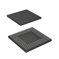
D17760BP200ADV Renesas Electronics America, D17760BP200ADV Datasheet - Page 68

D17760BP200ADV
Manufacturer Part Number
D17760BP200ADV
Description
MPU 3V 8K,PB-FREE, 256-BGA
Manufacturer
Renesas Electronics America
Series
SuperH® SH7750r
Datasheet
1.D6417760BP200ADV.pdf
(1418 pages)
Specifications of D17760BP200ADV
Core Processor
SH-4
Core Size
32-Bit
Speed
200MHz
Connectivity
Audio Codec, CAN, EBI/EMI, FIFO, I²C, MFI, MMC, SCI, Serial Sound, SIM, SPI, USB
Peripherals
DMA, LCD, POR, WDT
Number Of I /o
69
Program Memory Type
ROMless
Ram Size
48K x 8
Voltage - Supply (vcc/vdd)
1.4 V ~ 1.6 V
Data Converters
A/D 4x10b
Oscillator Type
Internal
Operating Temperature
-40°C ~ 85°C
Package / Case
256-BGA
Lead Free Status / RoHS Status
Lead free / RoHS Compliant
Eeprom Size
-
Program Memory Size
-
Available stocks
Company
Part Number
Manufacturer
Quantity
Price
Company:
Part Number:
D17760BP200ADV
Manufacturer:
Renesas Electronics America
Quantity:
10 000
- Current page: 68 of 1418
- Download datasheet (9Mb)
Figure 17.22 Receive Data Sampling Timing in Asynchronous Mode ....................................... 625
Figure 17.23 Example of Synchronization Clock Transfer by DMAC ....................................... 626
Section 18 SIM Card Module (SIM)
Figure 18.1 Block Diagram of SIM........................................................................................... 628
Figure 18.2 Data Format Used by the Smart Card Interface ..................................................... 648
Figure 18.3 Examples of Initial Character Waveforms ............................................................. 650
Figure 18.4 Example of Initialization Flow............................................................................... 652
Figure 18.5 Example of Transmission Processing..................................................................... 653
Figure 18.6 Example of Reception Processing .......................................................................... 654
Figure 18.7 Received Data Sampling Timing in Smart Card Mode.......................................... 657
Figure 18.8 Repetition in the Smart Card Interface Receiver Mode.......................................... 657
Figure 18.9 Repetition Standby Mode (clock stopped) when the Smart Card Interface Is in
Figure 18.10 TEIE Set Timing .................................................................................................... 659
Figure 18.11 Procedure for Stopping the Clock and Restarting .................................................. 660
Figure 18.12 Example of Smart Card Interface Pin Connections................................................ 661
Section 19 I
Figure 19.1 I
Figure 19.2 I
Figure 19.3 Master Data Transmit format ................................................................................. 691
Figure 19.4 Master Data Receive format................................................................................... 691
Figure 19.5 Combination Transfer Format of Master Transfer ................................................. 691
Figure 19.6 10-Bit Address Data Transfer Format .................................................................... 692
Figure 19.7 10-Bit Address Data Receive Format..................................................................... 692
Figure 19.8 10-Bit Address Transmit/Receive Combination Format ........................................ 693
Figure 19.9 Data Transfer Mode Timing Chart ......................................................................... 695
Figure 19.10 Data Receive Mode Timing Chart.......................................................................... 696
Figure 19.11 Period for Setting FSB = 1 for which a Stop Condition (P) will be Correctly
Section 20 Serial Sound Interface (SSI) Module
Figure 20.1 Block Diagram of SSI Module............................................................................... 708
Figure 20.2 Philips Format (with no Padding) .......................................................................... 724
Figure 20.3 Philips Format (with Padding) ............................................................................... 724
Figure 20.4 Sony Format (with Serial Data First, Followed by Padding Bits) .......................... 725
Figure 20.5 Matsushita Format (with Padding Bits First, Followed by Serial Data)................. 725
Figure 20.6 Multichannel Format (4 Channels, No Padding).................................................... 727
Figure 20.7 Multichannel Format (6 Channels with High Padding).......................................... 727
Figure 20.8 Multichannel Format (8 Channels, with Padding Bits First, Followed by
Rev. 2.00 Feb. 12, 2010 Page lxvi of lxxxii
REJ09B0554-0200
Transmitter Mode................................................................................................... 658
Issued ..................................................................................................................... 705
Serial Data, with Padding)...................................................................................... 728
2
2
2
C Bus Interface
C Bus Interface Block Diagram ........................................................................... 663
C Bus Timing....................................................................................................... 690
Related parts for D17760BP200ADV
Image
Part Number
Description
Manufacturer
Datasheet
Request
R

Part Number:
Description:
KIT STARTER FOR M16C/29
Manufacturer:
Renesas Electronics America
Datasheet:

Part Number:
Description:
KIT STARTER FOR R8C/2D
Manufacturer:
Renesas Electronics America
Datasheet:

Part Number:
Description:
R0K33062P STARTER KIT
Manufacturer:
Renesas Electronics America
Datasheet:

Part Number:
Description:
KIT STARTER FOR R8C/23 E8A
Manufacturer:
Renesas Electronics America
Datasheet:

Part Number:
Description:
KIT STARTER FOR R8C/25
Manufacturer:
Renesas Electronics America
Datasheet:

Part Number:
Description:
KIT STARTER H8S2456 SHARPE DSPLY
Manufacturer:
Renesas Electronics America
Datasheet:

Part Number:
Description:
KIT STARTER FOR R8C38C
Manufacturer:
Renesas Electronics America
Datasheet:

Part Number:
Description:
KIT STARTER FOR R8C35C
Manufacturer:
Renesas Electronics America
Datasheet:

Part Number:
Description:
KIT STARTER FOR R8CL3AC+LCD APPS
Manufacturer:
Renesas Electronics America
Datasheet:

Part Number:
Description:
KIT STARTER FOR RX610
Manufacturer:
Renesas Electronics America
Datasheet:

Part Number:
Description:
KIT STARTER FOR R32C/118
Manufacturer:
Renesas Electronics America
Datasheet:

Part Number:
Description:
KIT DEV RSK-R8C/26-29
Manufacturer:
Renesas Electronics America
Datasheet:

Part Number:
Description:
KIT STARTER FOR SH7124
Manufacturer:
Renesas Electronics America
Datasheet:

Part Number:
Description:
KIT STARTER FOR H8SX/1622
Manufacturer:
Renesas Electronics America
Datasheet:

Part Number:
Description:
KIT DEV FOR SH7203
Manufacturer:
Renesas Electronics America
Datasheet:


