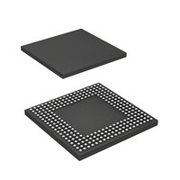
D17760BP200ADV Renesas Electronics America, D17760BP200ADV Datasheet - Page 523

D17760BP200ADV
Manufacturer Part Number
D17760BP200ADV
Description
MPU 3V 8K,PB-FREE, 256-BGA
Manufacturer
Renesas Electronics America
Series
SuperH® SH7750r
Datasheet
1.D6417760BP200ADV.pdf
(1418 pages)
Specifications of D17760BP200ADV
Core Processor
SH-4
Core Size
32-Bit
Speed
200MHz
Connectivity
Audio Codec, CAN, EBI/EMI, FIFO, I²C, MFI, MMC, SCI, Serial Sound, SIM, SPI, USB
Peripherals
DMA, LCD, POR, WDT
Number Of I /o
69
Program Memory Type
ROMless
Ram Size
48K x 8
Voltage - Supply (vcc/vdd)
1.4 V ~ 1.6 V
Data Converters
A/D 4x10b
Oscillator Type
Internal
Operating Temperature
-40°C ~ 85°C
Package / Case
256-BGA
Lead Free Status / RoHS Status
Lead free / RoHS Compliant
Eeprom Size
-
Program Memory Size
-
Available stocks
Company
Part Number
Manufacturer
Quantity
Price
Company:
Part Number:
D17760BP200ADV
Manufacturer:
Renesas Electronics America
Quantity:
10 000
- Current page: 523 of 1418
- Download datasheet (9Mb)
1
2
3
4
5
6
Table 11.9 (2)
Legend:
O: DACK output setting in dual address mode transfer
Notes: 1. SRAM-type in the table indicates an SRAM, byte control SRAM, or burst ROM.
(4) Bus Mode and Channel Priority Order
When, for example, channel 1 is transferring data in burst mode, and a transfer request is issued to
channel 0, which has a higher priority, the channel 0 transfer is started immediately.
If fixed mode has been set for the priority levels (CH0 > CH1), transfer on channel 1 is continued
after transfer on channel 0 is completely finished, whether cycle steal mode or burst mode is set
for channel 0.
If round robin mode has been set for the priority levels, transfer on channel 1 is restarted after one
transfer unit of data is transferred on channel 0, whether cycle steal mode or burst mode is set for
channel 0. Channel execution alternates in the order: channel 1 → channel 0 → channel 1 →
channel 0.
An example of round robin mode operation is shown in figure 11.12.
Since channel 1 is in burst mode (in the case of edge sensing) regardless of whether fixed mode or
round robin mode is set for the priority order, the bus is not released to the CPU until channel 1
transfer ends.
Synchronous DRAM
External device with DACK
Synchronous DRAM
SRAM-type, MPX, PCMCIA
SRAM-type, PCMCIA, MPX
SRAM-type, MPX, PCMCIA
Transfer Source
2. Memory interface in which transfer is possible in single address mode is synchronous
3. When performing dual address mode transfer, make the DACK output setting for the
DRAM.
SRAM, byte control SRAM, burst ROM, PCMCIA, or MPX interface.
Transfer Direction (Settable Memory Interface)
External Request Transfer Sources and Destinations in DMABRG Mode
O Synchronous DRAM
O SRAM-type, PCMCIA, MPX
External device with DACK
Synchronous DRAM
SRAM-type, MPX, PCMCIA
SRAM-type, MPX, PCMCIA
Transfer Destination
Rev. 2.00 Feb. 12, 2010 Page 439 of 1330
O Dual
O Dual
Single
Single
Dual
Address
Mode
Dual
REJ09B0554-0200
All
All
All
All
Usable
DMAC
Channels
All
All
Related parts for D17760BP200ADV
Image
Part Number
Description
Manufacturer
Datasheet
Request
R

Part Number:
Description:
KIT STARTER FOR M16C/29
Manufacturer:
Renesas Electronics America
Datasheet:

Part Number:
Description:
KIT STARTER FOR R8C/2D
Manufacturer:
Renesas Electronics America
Datasheet:

Part Number:
Description:
R0K33062P STARTER KIT
Manufacturer:
Renesas Electronics America
Datasheet:

Part Number:
Description:
KIT STARTER FOR R8C/23 E8A
Manufacturer:
Renesas Electronics America
Datasheet:

Part Number:
Description:
KIT STARTER FOR R8C/25
Manufacturer:
Renesas Electronics America
Datasheet:

Part Number:
Description:
KIT STARTER H8S2456 SHARPE DSPLY
Manufacturer:
Renesas Electronics America
Datasheet:

Part Number:
Description:
KIT STARTER FOR R8C38C
Manufacturer:
Renesas Electronics America
Datasheet:

Part Number:
Description:
KIT STARTER FOR R8C35C
Manufacturer:
Renesas Electronics America
Datasheet:

Part Number:
Description:
KIT STARTER FOR R8CL3AC+LCD APPS
Manufacturer:
Renesas Electronics America
Datasheet:

Part Number:
Description:
KIT STARTER FOR RX610
Manufacturer:
Renesas Electronics America
Datasheet:

Part Number:
Description:
KIT STARTER FOR R32C/118
Manufacturer:
Renesas Electronics America
Datasheet:

Part Number:
Description:
KIT DEV RSK-R8C/26-29
Manufacturer:
Renesas Electronics America
Datasheet:

Part Number:
Description:
KIT STARTER FOR SH7124
Manufacturer:
Renesas Electronics America
Datasheet:

Part Number:
Description:
KIT STARTER FOR H8SX/1622
Manufacturer:
Renesas Electronics America
Datasheet:

Part Number:
Description:
KIT DEV FOR SH7203
Manufacturer:
Renesas Electronics America
Datasheet:


