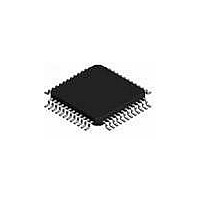
MC68908GZ8MFAE Freescale Semiconductor, MC68908GZ8MFAE Datasheet - Page 133

MC68908GZ8MFAE
Manufacturer Part Number
MC68908GZ8MFAE
Description
IC MCU 8BIT 8K FLASH 48-LQFP
Manufacturer
Freescale Semiconductor
Series
HC08r
Datasheet
1.MC68908GZ8CFJER.pdf
(314 pages)
Specifications of MC68908GZ8MFAE
Core Processor
HC08
Core Size
8-Bit
Speed
8MHz
Connectivity
CAN, LIN, SCI, SPI
Peripherals
LVD, POR, PWM
Number Of I /o
37
Program Memory Size
8KB (8K x 8)
Program Memory Type
FLASH
Ram Size
1K x 8
Voltage - Supply (vcc/vdd)
3 V ~ 5.5 V
Data Converters
A/D 8x10b
Oscillator Type
Internal
Operating Temperature
-40°C ~ 125°C
Package / Case
48-LQFP
Processor Series
M689xx
Core
HC08
Data Bus Width
8 bit
Data Ram Size
1 KB
Interface Type
SPI, SCI, CAN
Maximum Clock Frequency
8 MHz
Number Of Programmable I/os
37
Number Of Timers
2
Operating Supply Voltage
5.5 V
Maximum Operating Temperature
+ 125 C
Mounting Style
SMD/SMT
Development Tools By Supplier
FSICEBASE, M68CBL05AE, DEMO908GZ60E, M68EML08GZE
Minimum Operating Temperature
- 40 C
On-chip Adc
10 bit, 16 Channel
Lead Free Status / RoHS Status
Lead free / RoHS Compliant
Eeprom Size
-
Lead Free Status / Rohs Status
Details
- Current page: 133 of 314
- Download datasheet (5Mb)
Timer Link
To protect the CAN bus system from fatal consequences resulting from violations of the above rule, the
MSCAN08 drives the CAN
pin into recessive state.
TX
In power-down mode, no registers can be accessed.
MSCAN08 bus activity can wake the MCU from CPU stop/MSCAN08 power-down mode. However, until
the oscillator starts up and synchronization is achieved the MSCAN08 will not respond to incoming data.
12.8.4 CPU Wait Mode
The MSCAN08 module remains active during CPU wait mode. The MSCAN08 will stay synchronized to
the CAN bus and generates transmit, receive, and error interrupts to the CPU, if enabled. Any such
interrupt will bring the MCU out of wait mode.
12.8.5 Programmable Wakeup Function
The MSCAN08 can be programmed to apply a low-pass filter function to the CAN
input line while in
RX
internal sleep mode (see information on control bit WUPM in
12.13.2 MSCAN08 Module Control Register
1). This feature can be used to protect the MSCAN08 from wakeup due to short glitches on the CAN bus
lines. Such glitches can result from electromagnetic inference within noisy environments.
12.9 Timer Link
The MSCAN08 will generate a timer signal whenever a valid frame has been received. Because the CAN
specification defines a frame to be valid if no errors occurred before the EOF field has been transmitted
successfully, the timer signal will be generated right after the EOF. A pulse of one bit time is generated.
As the MSCAN08 receiver engine also receives the frames being sent by itself, a timer signal also will be
generated after a successful transmission.
The previously described timer signal can be routed into the on-chip timer interface module (TIM). This
signal is connected to channel 0 of timer interface module 1 (TIM1) under the control of the timer link
enable (TLNKEN) bit in CMCR0.
After the timer has been programmed to capture rising edge events, it can be used under software control
to generate 16-bit time stamps which can be stored with the received message.
12.10 Clock System
Figure 12-8
shows the structure of the MSCAN08 clock generation circuitry and its interaction with the
clock generation module (CGM). With this flexible clocking scheme the MSCAN08 is able to handle CAN
bus rates ranging from 10 kbps up to 1 Mbps.
The clock source bit (CLKSRC) in the MSCAN08 module control register (CMCR1) (see
12.13.1
MSCAN08 Module Control Register
0) defines whether the MSCAN08 is connected to the output of the
crystal oscillator or to the PLL output.
The clock source has to be chosen such that the tight oscillator tolerance requirements (up to 0.4%) of
the CAN protocol are met.
MC68HC908GZ16 • MC68HC908GZ8 Data Sheet, Rev. 4
Freescale Semiconductor
133
Related parts for MC68908GZ8MFAE
Image
Part Number
Description
Manufacturer
Datasheet
Request
R
Part Number:
Description:
Manufacturer:
Freescale Semiconductor, Inc
Datasheet:
Part Number:
Description:
Manufacturer:
Freescale Semiconductor, Inc
Datasheet:
Part Number:
Description:
Manufacturer:
Freescale Semiconductor, Inc
Datasheet:
Part Number:
Description:
Manufacturer:
Freescale Semiconductor, Inc
Datasheet:
Part Number:
Description:
Manufacturer:
Freescale Semiconductor, Inc
Datasheet:
Part Number:
Description:
Manufacturer:
Freescale Semiconductor, Inc
Datasheet:
Part Number:
Description:
Manufacturer:
Freescale Semiconductor, Inc
Datasheet:
Part Number:
Description:
Manufacturer:
Freescale Semiconductor, Inc
Datasheet:
Part Number:
Description:
Manufacturer:
Freescale Semiconductor, Inc
Datasheet:
Part Number:
Description:
Manufacturer:
Freescale Semiconductor, Inc
Datasheet:
Part Number:
Description:
Manufacturer:
Freescale Semiconductor, Inc
Datasheet:
Part Number:
Description:
Manufacturer:
Freescale Semiconductor, Inc
Datasheet:
Part Number:
Description:
Manufacturer:
Freescale Semiconductor, Inc
Datasheet:
Part Number:
Description:
Manufacturer:
Freescale Semiconductor, Inc
Datasheet:
Part Number:
Description:
Manufacturer:
Freescale Semiconductor, Inc
Datasheet:


