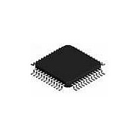
MC68908GZ8MFAE Freescale Semiconductor, MC68908GZ8MFAE Datasheet - Page 74

MC68908GZ8MFAE
Manufacturer Part Number
MC68908GZ8MFAE
Description
IC MCU 8BIT 8K FLASH 48-LQFP
Manufacturer
Freescale Semiconductor
Series
HC08r
Datasheet
1.MC68908GZ8CFJER.pdf
(314 pages)
Specifications of MC68908GZ8MFAE
Core Processor
HC08
Core Size
8-Bit
Speed
8MHz
Connectivity
CAN, LIN, SCI, SPI
Peripherals
LVD, POR, PWM
Number Of I /o
37
Program Memory Size
8KB (8K x 8)
Program Memory Type
FLASH
Ram Size
1K x 8
Voltage - Supply (vcc/vdd)
3 V ~ 5.5 V
Data Converters
A/D 8x10b
Oscillator Type
Internal
Operating Temperature
-40°C ~ 125°C
Package / Case
48-LQFP
Processor Series
M689xx
Core
HC08
Data Bus Width
8 bit
Data Ram Size
1 KB
Interface Type
SPI, SCI, CAN
Maximum Clock Frequency
8 MHz
Number Of Programmable I/os
37
Number Of Timers
2
Operating Supply Voltage
5.5 V
Maximum Operating Temperature
+ 125 C
Mounting Style
SMD/SMT
Development Tools By Supplier
FSICEBASE, M68CBL05AE, DEMO908GZ60E, M68EML08GZE
Minimum Operating Temperature
- 40 C
On-chip Adc
10 bit, 16 Channel
Lead Free Status / RoHS Status
Lead free / RoHS Compliant
Eeprom Size
-
Lead Free Status / Rohs Status
Details
- Current page: 74 of 314
- Download datasheet (5Mb)
Clock Generator Module (CGM)
VRS7–VRS0 — VCO Range Select Bits
4.6 Interrupts
When the AUTO bit is set in the PLL bandwidth control register (PBWC), the PLL can generate a CPU
interrupt request every time the LOCK bit changes state. The PLLIE bit in the PLL control register (PCTL)
enables CPU interrupts from the PLL. PLLF, the interrupt flag in the PCTL, becomes set whether
interrupts are enabled or not. When the AUTO bit is clear, CPU interrupts from the PLL are disabled and
PLLF reads as logic 0.
Software should read the LOCK bit after a PLL interrupt request to see if the request was due to an entry
into lock or an exit from lock. When the PLL enters lock, the VCO clock, CGMVCLK, divided by two can
be selected as the CGMOUT source by setting BCS in the PCTL. When the PLL exits lock, the VCO clock
frequency is corrupt, and appropriate precautions should be taken. If the application is not frequency
sensitive, interrupts should be disabled to prevent PLL interrupt service routines from impeding software
performance or from exceeding stack limitations.
74
These read/write bits control the hardware center-of-range linear multiplier L which, in conjunction with
E (See
hardware center-of-range frequency, f
PCTL is set. (See
register disables the PLL and clears the BCS bit in the PLL control register (PCTL). (See
Clock Selector Circuit
for a default range multiply value of 64.
4.3.3 PLL
Verify that the value of the PMRS register is appropriate for the given
reference and VCO clock frequencies before enabling the PLL. See
Programming the PLL
for these control bits.
The VCO range select bits have built-in protection such that they cannot be
written when the PLL is on (PLLON = 1) and such that the VCO clock
cannot be selected as the source of the base clock (BCS = 1) if the VCO
range select bits are all clear.
The PLL VCO range select register must be programmed correctly.
Incorrect programming can result in failure of the PLL to achieve lock.
Software can select the CGMVCLK divided by two as the CGMOUT source
even if the PLL is not locked (LOCK = 0). Therefore, software should make
sure the PLL is locked before setting the BCS bit.
Circuits,
4.3.7 Special Programming
and
MC68HC908GZ16 • MC68HC908GZ8 Data Sheet, Rev. 4
4.3.7 Special Programming
4.3.6 Programming the
for detailed instructions on selecting the proper value
VRS
. VRS7–VRS0 cannot be written when the PLLON bit in the
NOTE
NOTE
NOTE
Exceptions.) A value of $00 in the VCO range select
PLL, and
Exceptions.). Reset initializes the register to $40
4.5.1 PLL Control
Register.), controls the
Freescale Semiconductor
4.3.6
4.3.8 Base
Related parts for MC68908GZ8MFAE
Image
Part Number
Description
Manufacturer
Datasheet
Request
R
Part Number:
Description:
Manufacturer:
Freescale Semiconductor, Inc
Datasheet:
Part Number:
Description:
Manufacturer:
Freescale Semiconductor, Inc
Datasheet:
Part Number:
Description:
Manufacturer:
Freescale Semiconductor, Inc
Datasheet:
Part Number:
Description:
Manufacturer:
Freescale Semiconductor, Inc
Datasheet:
Part Number:
Description:
Manufacturer:
Freescale Semiconductor, Inc
Datasheet:
Part Number:
Description:
Manufacturer:
Freescale Semiconductor, Inc
Datasheet:
Part Number:
Description:
Manufacturer:
Freescale Semiconductor, Inc
Datasheet:
Part Number:
Description:
Manufacturer:
Freescale Semiconductor, Inc
Datasheet:
Part Number:
Description:
Manufacturer:
Freescale Semiconductor, Inc
Datasheet:
Part Number:
Description:
Manufacturer:
Freescale Semiconductor, Inc
Datasheet:
Part Number:
Description:
Manufacturer:
Freescale Semiconductor, Inc
Datasheet:
Part Number:
Description:
Manufacturer:
Freescale Semiconductor, Inc
Datasheet:
Part Number:
Description:
Manufacturer:
Freescale Semiconductor, Inc
Datasheet:
Part Number:
Description:
Manufacturer:
Freescale Semiconductor, Inc
Datasheet:
Part Number:
Description:
Manufacturer:
Freescale Semiconductor, Inc
Datasheet:


