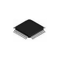
MC68908GZ8MFAE Freescale Semiconductor, MC68908GZ8MFAE Datasheet - Page 250

MC68908GZ8MFAE
Manufacturer Part Number
MC68908GZ8MFAE
Description
IC MCU 8BIT 8K FLASH 48-LQFP
Manufacturer
Freescale Semiconductor
Series
HC08r
Datasheet
1.MC68908GZ8CFJER.pdf
(314 pages)
Specifications of MC68908GZ8MFAE
Core Processor
HC08
Core Size
8-Bit
Speed
8MHz
Connectivity
CAN, LIN, SCI, SPI
Peripherals
LVD, POR, PWM
Number Of I /o
37
Program Memory Size
8KB (8K x 8)
Program Memory Type
FLASH
Ram Size
1K x 8
Voltage - Supply (vcc/vdd)
3 V ~ 5.5 V
Data Converters
A/D 8x10b
Oscillator Type
Internal
Operating Temperature
-40°C ~ 125°C
Package / Case
48-LQFP
Processor Series
M689xx
Core
HC08
Data Bus Width
8 bit
Data Ram Size
1 KB
Interface Type
SPI, SCI, CAN
Maximum Clock Frequency
8 MHz
Number Of Programmable I/os
37
Number Of Timers
2
Operating Supply Voltage
5.5 V
Maximum Operating Temperature
+ 125 C
Mounting Style
SMD/SMT
Development Tools By Supplier
FSICEBASE, M68CBL05AE, DEMO908GZ60E, M68EML08GZE
Minimum Operating Temperature
- 40 C
On-chip Adc
10 bit, 16 Channel
Lead Free Status / RoHS Status
Lead free / RoHS Compliant
Eeprom Size
-
Lead Free Status / Rohs Status
Details
- Current page: 250 of 314
- Download datasheet (5Mb)
Serial Peripheral Interface (SPI) Module
MODFEN — Mode Fault Enable Bit
SPR1 and SPR0 — SPI Baud Rate Select Bits
17.13.3 SPI Data Register
The SPI data register consists of the read-only receive data register and the write-only transmit data
register. Writing to the SPI data register writes data into the transmit data register. Reading the SPI data
register reads data from the receive data register. The transmit data and receive data registers are
separate registers that can contain different values. See
R7–R0/T7–T0 — Receive/Transmit Data Bits
250
This read/write bit, when set to 1, allows the MODF flag to be set. If the MODF flag is set, clearing the
MODFEN does not clear the MODF flag. If the SPI is enabled as a master and the MODFEN bit is low,
then the SS pin is available as a general-purpose I/O.
If the MODFEN bit is set, then this pin is not available as a general-purpose I/O. When the SPI is
enabled as a slave, the SS pin is not available as a general-purpose I/O regardless of the value of
MODFEN. See
If the MODFEN bit is low, the level of the SS pin does not affect the operation of an enabled SPI
configured as a master. For an enabled SPI configured as a slave, having MODFEN low only prevents
the MODF flag from being set. It does not affect any other part of SPI operation. See
Error.
In master mode, these read/write bits select one of four baud rates as shown in
SPR0 have no effect in slave mode. Reset clears SPR1 and SPR0.
Use this formula to calculate the SPI baud rate:
where:
CGMOUT = base clock output of the clock generator module (CGM)
BD = baud rate divisor
Address: $0012
Do not use read-modify-write instructions on the SPI data register since the
register read is not the same as the register written.
Reset:
Read:
Write:
17.12.4 SS (Slave Select).
Bit 7
R7
T7
MC68HC908GZ16 • MC68HC908GZ8 Data Sheet, Rev. 4
Table 17-4. SPI Master Baud Rate Selection
Baud rate
SPR1 and SPR0
Figure 17-16. SPI Data Register (SPDR)
R6
T6
6
00
01
10
11
=
R5
T5
5
CGMOUT
------------------------- -
2
×
BD
NOTE
Unaffected by reset
R4
T4
4
Baud Rate Divisor (BD)
Figure
R3
T3
3
17-3.
128
32
2
8
R2
T2
2
R1
T1
1
Table
Freescale Semiconductor
17.7.2 Mode Fault
Bit 0
R0
T0
17-4. SPR1 and
Related parts for MC68908GZ8MFAE
Image
Part Number
Description
Manufacturer
Datasheet
Request
R
Part Number:
Description:
Manufacturer:
Freescale Semiconductor, Inc
Datasheet:
Part Number:
Description:
Manufacturer:
Freescale Semiconductor, Inc
Datasheet:
Part Number:
Description:
Manufacturer:
Freescale Semiconductor, Inc
Datasheet:
Part Number:
Description:
Manufacturer:
Freescale Semiconductor, Inc
Datasheet:
Part Number:
Description:
Manufacturer:
Freescale Semiconductor, Inc
Datasheet:
Part Number:
Description:
Manufacturer:
Freescale Semiconductor, Inc
Datasheet:
Part Number:
Description:
Manufacturer:
Freescale Semiconductor, Inc
Datasheet:
Part Number:
Description:
Manufacturer:
Freescale Semiconductor, Inc
Datasheet:
Part Number:
Description:
Manufacturer:
Freescale Semiconductor, Inc
Datasheet:
Part Number:
Description:
Manufacturer:
Freescale Semiconductor, Inc
Datasheet:
Part Number:
Description:
Manufacturer:
Freescale Semiconductor, Inc
Datasheet:
Part Number:
Description:
Manufacturer:
Freescale Semiconductor, Inc
Datasheet:
Part Number:
Description:
Manufacturer:
Freescale Semiconductor, Inc
Datasheet:
Part Number:
Description:
Manufacturer:
Freescale Semiconductor, Inc
Datasheet:
Part Number:
Description:
Manufacturer:
Freescale Semiconductor, Inc
Datasheet:


