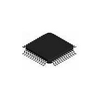
MC68908GZ8MFAE Freescale Semiconductor, MC68908GZ8MFAE Datasheet - Page 195

MC68908GZ8MFAE
Manufacturer Part Number
MC68908GZ8MFAE
Description
IC MCU 8BIT 8K FLASH 48-LQFP
Manufacturer
Freescale Semiconductor
Series
HC08r
Datasheet
1.MC68908GZ8CFJER.pdf
(314 pages)
Specifications of MC68908GZ8MFAE
Core Processor
HC08
Core Size
8-Bit
Speed
8MHz
Connectivity
CAN, LIN, SCI, SPI
Peripherals
LVD, POR, PWM
Number Of I /o
37
Program Memory Size
8KB (8K x 8)
Program Memory Type
FLASH
Ram Size
1K x 8
Voltage - Supply (vcc/vdd)
3 V ~ 5.5 V
Data Converters
A/D 8x10b
Oscillator Type
Internal
Operating Temperature
-40°C ~ 125°C
Package / Case
48-LQFP
Processor Series
M689xx
Core
HC08
Data Bus Width
8 bit
Data Ram Size
1 KB
Interface Type
SPI, SCI, CAN
Maximum Clock Frequency
8 MHz
Number Of Programmable I/os
37
Number Of Timers
2
Operating Supply Voltage
5.5 V
Maximum Operating Temperature
+ 125 C
Mounting Style
SMD/SMT
Development Tools By Supplier
FSICEBASE, M68CBL05AE, DEMO908GZ60E, M68EML08GZE
Minimum Operating Temperature
- 40 C
On-chip Adc
10 bit, 16 Channel
Lead Free Status / RoHS Status
Lead free / RoHS Compliant
Eeprom Size
-
Lead Free Status / Rohs Status
Details
- Current page: 195 of 314
- Download datasheet (5Mb)
15.5 Low-Power Modes
The WAIT and STOP instructions put the MCU in low power-consumption standby modes.
15.5.1 Wait Mode
The ESCI module remains active in wait mode. Any enabled CPU interrupt request from the ESCI module
can bring the MCU out of wait mode.
If ESCI module functions are not required during wait mode, reduce power consumption by disabling the
module before executing the WAIT instruction.
15.5.2 Stop Mode
The ESCI module is inactive in stop mode. The STOP instruction does not affect ESCI register states.
ESCI module operation resumes after the MCU exits stop mode.
Because the internal clock is inactive during stop mode, entering stop mode during an ESCI transmission
or reception results in invalid data.
15.6 ESCI During Break Module Interrupts
The BCFE bit in the break flag control register (SBFCR) enables software to clear status bits during the
break state. See
To allow software to clear status bits during a break interrupt, write a logic 1 to the BCFE bit. If a status
bit is cleared during the break state, it remains cleared when the MCU exits the break state.
To protect status bits during the break state, write a logic 0 to the BCFE bit. With BCFE at logic 0 (its
default state), software can read and write I/O registers during the break state without affecting status bits.
Some status bits have a two-step read/write clearing procedure. If software does the first step on such a
bit before the break, the bit cannot change during the break state as long as BCFE is at logic 0. After the
break, doing the second step clears the status bit.
15.7 I/O Signals
Port E shares two of its pins with the ESCI module. The two ESCI I/O pins are:
15.7.1 PTE0/TxD (Transmit Data)
The PTE0/TxD pin is the serial data output from the ESCI transmitter. The ESCI shares the PTE0/TxD
pin with port E. When the ESCI is enabled, the PTE0/TxD pin is an output regardless of the state of the
DDRE0 bit in data direction register E (DDRE).
15.7.2 PTE1/RxD (Receive Data)
The PTE1/RxD pin is the serial data input to the ESCI receiver. The ESCI shares the PTE1/RxD pin with
port E. When the ESCI is enabled, the PTE1/RxD pin is an input regardless of the state of the DDRE1 bit
in data direction register E (DDRE).
Freescale Semiconductor
•
•
PTE0/TxD — transmit data
PTE1/RxD — receive data
Chapter 20 Development
MC68HC908GZ16 • MC68HC908GZ8 Data Sheet, Rev. 4
Support.
Low-Power Modes
195
Related parts for MC68908GZ8MFAE
Image
Part Number
Description
Manufacturer
Datasheet
Request
R
Part Number:
Description:
Manufacturer:
Freescale Semiconductor, Inc
Datasheet:
Part Number:
Description:
Manufacturer:
Freescale Semiconductor, Inc
Datasheet:
Part Number:
Description:
Manufacturer:
Freescale Semiconductor, Inc
Datasheet:
Part Number:
Description:
Manufacturer:
Freescale Semiconductor, Inc
Datasheet:
Part Number:
Description:
Manufacturer:
Freescale Semiconductor, Inc
Datasheet:
Part Number:
Description:
Manufacturer:
Freescale Semiconductor, Inc
Datasheet:
Part Number:
Description:
Manufacturer:
Freescale Semiconductor, Inc
Datasheet:
Part Number:
Description:
Manufacturer:
Freescale Semiconductor, Inc
Datasheet:
Part Number:
Description:
Manufacturer:
Freescale Semiconductor, Inc
Datasheet:
Part Number:
Description:
Manufacturer:
Freescale Semiconductor, Inc
Datasheet:
Part Number:
Description:
Manufacturer:
Freescale Semiconductor, Inc
Datasheet:
Part Number:
Description:
Manufacturer:
Freescale Semiconductor, Inc
Datasheet:
Part Number:
Description:
Manufacturer:
Freescale Semiconductor, Inc
Datasheet:
Part Number:
Description:
Manufacturer:
Freescale Semiconductor, Inc
Datasheet:
Part Number:
Description:
Manufacturer:
Freescale Semiconductor, Inc
Datasheet:


