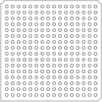
LFXP2-8E-5FTN256I Lattice, LFXP2-8E-5FTN256I Datasheet - Page 114

LFXP2-8E-5FTN256I
Manufacturer Part Number
LFXP2-8E-5FTN256I
Description
FPGA - Field Programmable Gate Array 8K LUTs 201 I/O Inst on DSP 1.2V -5 Spd
Manufacturer
Lattice
Datasheet
1.LFXP2-8E-5FTN256I.pdf
(341 pages)
Specifications of LFXP2-8E-5FTN256I
Number Of Macrocells
8000
Number Of Programmable I/os
201
Data Ram Size
226304
Supply Voltage (max)
1.26 V
Maximum Operating Temperature
+ 100 C
Minimum Operating Temperature
- 40 C
Mounting Style
SMD/SMT
Supply Voltage (min)
1.14 V
Package / Case
FTBGA-256
Number Of Logic Elements/cells
*
Number Of Labs/clbs
*
Total Ram Bits
226304
Number Of I /o
201
Number Of Gates
-
Voltage - Supply
1.14 V ~ 1.26 V
Mounting Type
*
Operating Temperature
-40°C ~ 100°C
Package
256FTBGA
Family Name
LatticeXP2
Device Logic Units
8000
Typical Operating Supply Voltage
1.2 V
Maximum Number Of User I/os
201
Ram Bits
226304
Re-programmability Support
Yes
Lead Free Status / RoHS Status
Lead free / RoHS Compliant
Available stocks
Company
Part Number
Manufacturer
Quantity
Price
Company:
Part Number:
LFXP2-8E-5FTN256I
Manufacturer:
Lattice Semiconductor Corporation
Quantity:
10 000
- Current page: 114 of 341
- Download datasheet (10Mb)
Lattice Semiconductor
FIXEDDELAY
The FIXEDDELAY attribute is available to each input pin. This attribute, when enabled, is used to achieve zero hold
time for the input registers when using global clock. This attribute can only be assigned in the HDL source.
Values: TRUE, FALSE
Default: FALSE
INBUF
By default, all the unused input buffers are disabled. The INBUF attribute is used to enable the unused input buffers
when performing a boundary scan test. This is a global attribute and can be globally set to ON or OFF.
Values: ON, OFF
Default: ON
DIN/DOUT
This attribute can be used to assign I/O registers. Using DIN will assert an input register and using the DOUT attri-
bute will assert an output register. By default, the software will try to assign the I/O registers, if applicable. The user
can turn this OFF by using the synthesis attribute or by using the Spreadsheet view of the Design Planner. These
attributes can only be applied to registers.
LOC
This attribute can be used to make pin assignments to the I/O ports in the design. This attributes is only used when
the pin assignments are made in HDL source. Designers can also assign pins directly using the Spreadsheet view
of the Design Planner in the ispLEVER software. The appendices explain this in further detail.
Design Considerations and Usage
This section discusses some of the design rules and considerations that must be taken into account when design-
ing with the LatticeXP2 sysIO buffer
Banking Rules
• If V
• If V
• When implementing DDR memory interfaces, the V
• Only the top and bottom banks (banks 0, 1, 4 and 5)) will support PCI clamps.
• All legal input buffers should be independent of bank V
Differential I/O Rules
• All banks can support LVDS input buffers. Only the banks on the right and left sides (Banks 2, 3, 6 and 7) will
• All banks support emulated differential buffers using external resistor pack and complementary LVCMOS drivers.
• Only 50% of the I/Os on the left and right sides can provide LVDS output buffer capability. LVDS can only be
V
V
pins and cannot be used to power any other referenced inputs.
bank V
support True Differential output buffers. The banks on all sides will support the LVDS input buffers. The user can
use emulated LVDS output buffers on these banks.
assigned to the TRUE pad. The ispLEVER design tool will automatically assign the other I/Os of the differential
pair to the complementary pad. Refer to the device data sheet to see the pin listings for all LVDS pairs.
CCAUX,
CC
CCIO
CCIO
, thus minimizing leakage.
CCIO
or V
or V
thus minimizing leakage.
of 1.8V and 1.5V.
CCJ
CCJ
for any bank is set to 3.3 V, it is recommended that it be connected to the same power supply as
for any bank is set to 1.2V, it is recommended that it be connected to the same power supply as
REF1
8-10
CCIO,
of the bank is used to provide reference to the interface
except for 1.8V and 1.5V buffers, which require a
LatticeXP2 sysIO Usage Guide
Related parts for LFXP2-8E-5FTN256I
Image
Part Number
Description
Manufacturer
Datasheet
Request
R

Part Number:
Description:
FPGA - Field Programmable Gate Array 8K LUTs 100I/O Inst- on DSP 1.2V -5 Spd
Manufacturer:
Lattice
Datasheet:

Part Number:
Description:
FPGA - Field Programmable Gate Array 8K LUTs 201I/O Inst- on DSP 1.2V -5 Spd
Manufacturer:
Lattice
Datasheet:

Part Number:
Description:
FPGA - Field Programmable Gate Array 8K LUTs 100 I/O Inst on DSP 1.2V -5 Spd
Manufacturer:
Lattice
Datasheet:

Part Number:
Description:
IC, LATTICEXP2 FPGA, 435MHZ, QFP-208
Manufacturer:
LATTICE SEMICONDUCTOR
Datasheet:

Part Number:
Description:
FPGA - Field Programmable Gate Array 8K LUTs 86I/O Inst- on DSP 1.2V -5 Spd
Manufacturer:
Lattice

Part Number:
Description:
FPGA - Field Programmable Gate Array 8K LUTs 201I/O Inst- on DSP 1.2V -7 Spd
Manufacturer:
Lattice
Datasheet:
Part Number:
Description:
FPGA LatticeXP2 Family 8000 Cells Flash Technology 1.2V 144-Pin TQFP
Manufacturer:
LATTICE SEMICONDUCTOR
Datasheet:

Part Number:
Description:
IC DSP 8KLUTS 146I/O 208PQFP
Manufacturer:
Lattice
Datasheet:

Part Number:
Description:
IC DSP 8KLUTS 100I/O 144TQFP
Manufacturer:
Lattice
Datasheet:

Part Number:
Description:
IC DSP 8KLUTS 86I/O 132CSBGA
Manufacturer:
Lattice
Datasheet:

Part Number:
Description:
IC DSP 8KLUTS 86I/O 132CSBGA
Manufacturer:
Lattice
Datasheet:

Part Number:
Description:
IC DSP 8KLUTS 146I/O 208PQFP
Manufacturer:
Lattice
Datasheet:

Part Number:
Description:
IC DSP 8KLUTS 201I/O 256FTBGA
Manufacturer:
Lattice
Datasheet:

Part Number:
Description:
IC FPGA 8KLUTS 86I/O 132-BGA
Manufacturer:
Lattice
Datasheet:

Part Number:
Description:
IC FPGA 8KLUTS 86I/O 132-BGA
Manufacturer:
Lattice
Datasheet:


