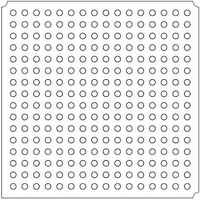
LFXP2-8E-5FTN256I Lattice, LFXP2-8E-5FTN256I Datasheet - Page 337

LFXP2-8E-5FTN256I
Manufacturer Part Number
LFXP2-8E-5FTN256I
Description
FPGA - Field Programmable Gate Array 8K LUTs 201 I/O Inst on DSP 1.2V -5 Spd
Manufacturer
Lattice
Datasheet
1.LFXP2-8E-5FTN256I.pdf
(341 pages)
Specifications of LFXP2-8E-5FTN256I
Number Of Macrocells
8000
Number Of Programmable I/os
201
Data Ram Size
226304
Supply Voltage (max)
1.26 V
Maximum Operating Temperature
+ 100 C
Minimum Operating Temperature
- 40 C
Mounting Style
SMD/SMT
Supply Voltage (min)
1.14 V
Package / Case
FTBGA-256
Number Of Logic Elements/cells
*
Number Of Labs/clbs
*
Total Ram Bits
226304
Number Of I /o
201
Number Of Gates
-
Voltage - Supply
1.14 V ~ 1.26 V
Mounting Type
*
Operating Temperature
-40°C ~ 100°C
Package
256FTBGA
Family Name
LatticeXP2
Device Logic Units
8000
Typical Operating Supply Voltage
1.2 V
Maximum Number Of User I/os
201
Ram Bits
226304
Re-programmability Support
Yes
Lead Free Status / RoHS Status
Lead free / RoHS Compliant
Available stocks
Company
Part Number
Manufacturer
Quantity
Price
Company:
Part Number:
LFXP2-8E-5FTN256I
Manufacturer:
Lattice Semiconductor Corporation
Quantity:
10 000
- Current page: 337 of 341
- Download datasheet (10Mb)
Lattice Semiconductor
Table 18-3. Configuration Pin Descriptions
JTAG Interface
The JTAG interface pins are referenced to V
port supplies from 1.2V to 3.3V. In cases where V
JTAG interface cable or tester can support I/O interface with the same I/O voltage standard.
I/O Interface and Critical Pins
There are eight I/O banks on every LatticeXP2 device. I/O Bank 7 contains the configuration pins and as such, the
configuration requirements should have the highest priority to determine the supply voltage levels for V
I/O Pin Assignments Around V
The V
ment must keep away the “noisy” I/O pins away from the BGA ball location that are identified as sensitive pins as
shown in Figure 18-1. In this case the sensitive pins would be one of the V
are generally defined to have the highest switching frequency, highest V
rates. For example, using the Figure 18-1 3x3 and 5x5 grid of ball locations, one can identify the “keep out” ball
locations for the potentially “noisy” signals. Note: In fpBGA and ftBGA packages, V
own pins; it is connected to the V
Figure 18-1. “Quiet” Pin Assignment Consideration for BGA Package
CFG0
CFG1
PROGRAMN Input, weak pull-up
INITN
DONE
CCLK
SISPI
SOSPI
CSSPISN
CSSPIN
Pin Name
CCPLL
provides a “quiet” supply for the internal PLLs. For the best PLL jitter performance, careful pin assign-
Bi-Directional Open Drain, weak pull-up
Input or Output
Input, weak pull-up
Input, weak pull-up
Input, weak pull-up
Bi-Directional Open Drain with weak pull-up or Active Drive
Input or Output
Input or Output
Output, tri-state, weak pull-up
CCAUX
5x5
5x5
5x5
5x5
5x5
I/O Type
CCPLL
pins. In this case, this discussion applies to the V
CCJ
5x5
3x3
3x3
3x3
5x5
. Typically, JTAG pins are referenced to 3.3V supply. V
CCJ
Sensitive
18-3
5x5
3x3
3x3
5x5
is connected to supplies other than 3.3V, validate that the
Pin
5x5
3x3
3x3
3x3
5x5
Dual-Purpose
Dual-Purpose
Dual-Purpose
Dual-Purpose
Dual-Purpose
Dual-Purpose
Dual-Purpose
Dual-Purpose
Dual-Purpose
Dedicated
LatticeXP2 Hardware Checklist
Pin Type
CCIO
CCPLL
5x5
5x5
5x5
5x5
5x5
standard and fastest output slew
supply pins. The “noisy” I/O pins
CCPLL
FPGA configuration mode
selection
FPGA Configuration
control and status signals
Configuration clock
SPI control and data
signals
CCAUX
is not provided from its
Description
pins.
CCJ
CCIO7
can sup-
.
Related parts for LFXP2-8E-5FTN256I
Image
Part Number
Description
Manufacturer
Datasheet
Request
R

Part Number:
Description:
FPGA - Field Programmable Gate Array 8K LUTs 100I/O Inst- on DSP 1.2V -5 Spd
Manufacturer:
Lattice
Datasheet:

Part Number:
Description:
FPGA - Field Programmable Gate Array 8K LUTs 201I/O Inst- on DSP 1.2V -5 Spd
Manufacturer:
Lattice
Datasheet:

Part Number:
Description:
FPGA - Field Programmable Gate Array 8K LUTs 100 I/O Inst on DSP 1.2V -5 Spd
Manufacturer:
Lattice
Datasheet:

Part Number:
Description:
IC, LATTICEXP2 FPGA, 435MHZ, QFP-208
Manufacturer:
LATTICE SEMICONDUCTOR
Datasheet:

Part Number:
Description:
FPGA - Field Programmable Gate Array 8K LUTs 86I/O Inst- on DSP 1.2V -5 Spd
Manufacturer:
Lattice

Part Number:
Description:
FPGA - Field Programmable Gate Array 8K LUTs 201I/O Inst- on DSP 1.2V -7 Spd
Manufacturer:
Lattice
Datasheet:
Part Number:
Description:
FPGA LatticeXP2 Family 8000 Cells Flash Technology 1.2V 144-Pin TQFP
Manufacturer:
LATTICE SEMICONDUCTOR
Datasheet:

Part Number:
Description:
IC DSP 8KLUTS 146I/O 208PQFP
Manufacturer:
Lattice
Datasheet:

Part Number:
Description:
IC DSP 8KLUTS 100I/O 144TQFP
Manufacturer:
Lattice
Datasheet:

Part Number:
Description:
IC DSP 8KLUTS 86I/O 132CSBGA
Manufacturer:
Lattice
Datasheet:

Part Number:
Description:
IC DSP 8KLUTS 86I/O 132CSBGA
Manufacturer:
Lattice
Datasheet:

Part Number:
Description:
IC DSP 8KLUTS 146I/O 208PQFP
Manufacturer:
Lattice
Datasheet:

Part Number:
Description:
IC DSP 8KLUTS 201I/O 256FTBGA
Manufacturer:
Lattice
Datasheet:

Part Number:
Description:
IC FPGA 8KLUTS 86I/O 132-BGA
Manufacturer:
Lattice
Datasheet:

Part Number:
Description:
IC FPGA 8KLUTS 86I/O 132-BGA
Manufacturer:
Lattice
Datasheet:


