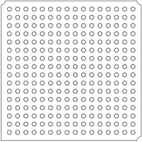
LFXP2-8E-5FTN256I Lattice, LFXP2-8E-5FTN256I Datasheet - Page 67

LFXP2-8E-5FTN256I
Manufacturer Part Number
LFXP2-8E-5FTN256I
Description
FPGA - Field Programmable Gate Array 8K LUTs 201 I/O Inst on DSP 1.2V -5 Spd
Manufacturer
Lattice
Datasheet
1.LFXP2-8E-5FTN256I.pdf
(341 pages)
Specifications of LFXP2-8E-5FTN256I
Number Of Macrocells
8000
Number Of Programmable I/os
201
Data Ram Size
226304
Supply Voltage (max)
1.26 V
Maximum Operating Temperature
+ 100 C
Minimum Operating Temperature
- 40 C
Mounting Style
SMD/SMT
Supply Voltage (min)
1.14 V
Package / Case
FTBGA-256
Number Of Logic Elements/cells
*
Number Of Labs/clbs
*
Total Ram Bits
226304
Number Of I /o
201
Number Of Gates
-
Voltage - Supply
1.14 V ~ 1.26 V
Mounting Type
*
Operating Temperature
-40°C ~ 100°C
Package
256FTBGA
Family Name
LatticeXP2
Device Logic Units
8000
Typical Operating Supply Voltage
1.2 V
Maximum Number Of User I/os
201
Ram Bits
226304
Re-programmability Support
Yes
Lead Free Status / RoHS Status
Lead free / RoHS Compliant
Available stocks
Company
Part Number
Manufacturer
Quantity
Price
Company:
Part Number:
LFXP2-8E-5FTN256I
Manufacturer:
Lattice Semiconductor Corporation
Quantity:
10 000
- Current page: 67 of 341
- Download datasheet (10Mb)
Lattice Semiconductor
RSDS
The LatticeXP2 devices support differential RSDS standard. This standard is emulated using complementary LVC-
MOS outputs in conjunction with a parallel resistor across the driver outputs. The RSDS input standard is sup-
ported by the LVDS differential input buffer. The scheme shown in Figure 3-4 is one possible solution for RSDS
standard implementation. Resistor values in Figure 3-4 are industry standard values for 1% resistors.
Figure 3-4. RSDS (Reduced Swing Differential Standard)
Table 3-4. RSDS DC Conditions
8mA
8mA
V CCIO = 2.5V
V CCIO = 2.5V
V
Z
R
R
R
V
V
V
V
Z
I
1. For input buffer, see LVDS table.
Parameter
DC
OUT
BACK
CCIO
OH
OL
OD
CM
S
P
T
On-chip
(+/-5%)
(+/-5%)
Output Driver Supply (+/-5%)
Driver Impedance
Driver Series Resistor (+/-1%)
Driver Parallel Resistor (+/-1%)
Receiver Termination (+/-1%)
Output High Voltage (After R
Output Low Voltage (After R
Output Differential Voltage (After R
Output Common Mode Voltage
Back Impedance
DC Output Current
1
Over Recommended Operating Conditions
R
R
S
S
Off-chip
= 294 ohms
= 294 ohms
(+/-1%)
(+/-1%)
Description
R
P
Zo = 100 ohm differential
= 121 ohms
(+/-1%)
3-12
Transmission line,
P
P
)
)
P
)
R
T
DC and Switching Characteristics
= 100 ohms
(+/-1%)
Typical
101.5
2.50
1.35
1.15
0.20
1.25
3.66
294
121
100
20
LatticeXP2 Family Data Sheet
Off-chip
Units
mA
V
V
V
V
V
On-chip
+
-
Related parts for LFXP2-8E-5FTN256I
Image
Part Number
Description
Manufacturer
Datasheet
Request
R

Part Number:
Description:
FPGA - Field Programmable Gate Array 8K LUTs 100I/O Inst- on DSP 1.2V -5 Spd
Manufacturer:
Lattice
Datasheet:

Part Number:
Description:
FPGA - Field Programmable Gate Array 8K LUTs 201I/O Inst- on DSP 1.2V -5 Spd
Manufacturer:
Lattice
Datasheet:

Part Number:
Description:
FPGA - Field Programmable Gate Array 8K LUTs 100 I/O Inst on DSP 1.2V -5 Spd
Manufacturer:
Lattice
Datasheet:

Part Number:
Description:
IC, LATTICEXP2 FPGA, 435MHZ, QFP-208
Manufacturer:
LATTICE SEMICONDUCTOR
Datasheet:

Part Number:
Description:
FPGA - Field Programmable Gate Array 8K LUTs 86I/O Inst- on DSP 1.2V -5 Spd
Manufacturer:
Lattice

Part Number:
Description:
FPGA - Field Programmable Gate Array 8K LUTs 201I/O Inst- on DSP 1.2V -7 Spd
Manufacturer:
Lattice
Datasheet:
Part Number:
Description:
FPGA LatticeXP2 Family 8000 Cells Flash Technology 1.2V 144-Pin TQFP
Manufacturer:
LATTICE SEMICONDUCTOR
Datasheet:

Part Number:
Description:
IC DSP 8KLUTS 146I/O 208PQFP
Manufacturer:
Lattice
Datasheet:

Part Number:
Description:
IC DSP 8KLUTS 100I/O 144TQFP
Manufacturer:
Lattice
Datasheet:

Part Number:
Description:
IC DSP 8KLUTS 86I/O 132CSBGA
Manufacturer:
Lattice
Datasheet:

Part Number:
Description:
IC DSP 8KLUTS 86I/O 132CSBGA
Manufacturer:
Lattice
Datasheet:

Part Number:
Description:
IC DSP 8KLUTS 146I/O 208PQFP
Manufacturer:
Lattice
Datasheet:

Part Number:
Description:
IC DSP 8KLUTS 201I/O 256FTBGA
Manufacturer:
Lattice
Datasheet:

Part Number:
Description:
IC FPGA 8KLUTS 86I/O 132-BGA
Manufacturer:
Lattice
Datasheet:

Part Number:
Description:
IC FPGA 8KLUTS 86I/O 132-BGA
Manufacturer:
Lattice
Datasheet:


