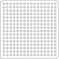
LFXP2-8E-5FTN256I Lattice, LFXP2-8E-5FTN256I Datasheet - Page 296

LFXP2-8E-5FTN256I
Manufacturer Part Number
LFXP2-8E-5FTN256I
Description
FPGA - Field Programmable Gate Array 8K LUTs 201 I/O Inst on DSP 1.2V -5 Spd
Manufacturer
Lattice
Datasheet
1.LFXP2-8E-5FTN256I.pdf
(341 pages)
Specifications of LFXP2-8E-5FTN256I
Number Of Macrocells
8000
Number Of Programmable I/os
201
Data Ram Size
226304
Supply Voltage (max)
1.26 V
Maximum Operating Temperature
+ 100 C
Minimum Operating Temperature
- 40 C
Mounting Style
SMD/SMT
Supply Voltage (min)
1.14 V
Package / Case
FTBGA-256
Number Of Logic Elements/cells
*
Number Of Labs/clbs
*
Total Ram Bits
226304
Number Of I /o
201
Number Of Gates
-
Voltage - Supply
1.14 V ~ 1.26 V
Mounting Type
*
Operating Temperature
-40°C ~ 100°C
Package
256FTBGA
Family Name
LatticeXP2
Device Logic Units
8000
Typical Operating Supply Voltage
1.2 V
Maximum Number Of User I/os
201
Ram Bits
226304
Re-programmability Support
Yes
Lead Free Status / RoHS Status
Lead free / RoHS Compliant
Available stocks
Company
Part Number
Manufacturer
Quantity
Price
Company:
Part Number:
LFXP2-8E-5FTN256I
Manufacturer:
Lattice Semiconductor Corporation
Quantity:
10 000
- Current page: 296 of 341
- Download datasheet (10Mb)
Lattice Semiconductor
LatticeXP2 sysCONFIG Usage Guide
Master Clock Frequency of 2.5 MHz. Some of the first bits in the configuration bitstream are MCCLK_FREQ, once
these are read the clock immediately starts operating at the user-defined frequency. The clock frequency is
changed using a glitchless switch. The default MCCLK frequency set in the bitstream is 3.1 MHz.
Security
When CONFIG_SECURE is set to ON, NO read back operation will be supported through the sysCONFIG or
ispJTAG port of the general contents. The ispJTAG DeviceID area is readable and not considered securable.
Default is OFF.
Wake Up Sequence
The WAKE_UP sequence controls three internal signals and the DONE pin. The DONE pin will be driven after con-
figuration and prior to user mode. See the Wake Up Sequence section of this document for an example of the
phase controls and information on the wake up selections. The default setting for the WAKE_UP preference is
determined by the DONE_EX setting.
Wake Up with DONE_EX = Off (Default Setting)
The WAKE_UP preference for DONE_EX = OFF (default) supports the user selectable options 1 through 25, as
shown in Table 14-6. If the user does not select a wake-up sequence, the default, for DONE_EX = OFF, will be
wake-up sequence 21.
Wake Up with DONE_EX = On
The WAKE_UP preference for DONE_EX = ON supports the user selectable options 1 through 7, as shown in
Table 14-6. If the user does not select a wake-up sequence, the default will be wake-up sequence 4.
Wake On Lock Selection
The Wake On Lock preference determines whether the device will wait for the PLL to lock before beginning the
wake-up process.
ON – The device will not wake up until the PLL lock signal for the given PLL is active.
OFF (default) – The device will wake up regardless of the state of the PLL lock signal.
Power Save
An I/O Power Save mode option, called INBUF, is used for the LatticeXP2 device and will deactivate unused input
buffers to save power. This is only affects comparator type inputs pins (pins that use VREF), like HSTL, SSTL, etc.
The Power Save mode limits some of the functionality of Boundary Scan. For Boundary Scan testing it is recom-
mended that the INBUF global preference be turned ON to activate all unused input buffers.
One Time Programmable Fuse
The LatticeXP2 has a One Time Programmable (OTP) fuse that can be used to prevent the on chip Flash configu-
ration memory from being erased or programmed. This does not prevent the Flash Tag Memory or Flash User
memory from being programmed, so these features are still available. The OTP fuse can be set using the Global
®
Configuration options in the ispLEVER Design Planner or it can be set directly using the ispVM
System software
at the time of download.
User GOE
The LatticeXP2 has a User GOE (Global Output Enable) feature. This allows the I/Os to be held in Boundary scan
control after the standard wake-up sequence has completed. User logic determines when the outputs get turned
over from Boundary Scan to User Logic control. This user logic input will be through a CIB and is valid for JTAG
“wake up” instructions only.
This feature is instantiated by the user as a macro called IOWAKEUP. This macro only has one signal and can only
be controlled immediately after the wakeup sequence (not anytime after).
14-14
Related parts for LFXP2-8E-5FTN256I
Image
Part Number
Description
Manufacturer
Datasheet
Request
R

Part Number:
Description:
FPGA - Field Programmable Gate Array 8K LUTs 100I/O Inst- on DSP 1.2V -5 Spd
Manufacturer:
Lattice
Datasheet:

Part Number:
Description:
FPGA - Field Programmable Gate Array 8K LUTs 201I/O Inst- on DSP 1.2V -5 Spd
Manufacturer:
Lattice
Datasheet:

Part Number:
Description:
FPGA - Field Programmable Gate Array 8K LUTs 100 I/O Inst on DSP 1.2V -5 Spd
Manufacturer:
Lattice
Datasheet:

Part Number:
Description:
IC, LATTICEXP2 FPGA, 435MHZ, QFP-208
Manufacturer:
LATTICE SEMICONDUCTOR
Datasheet:

Part Number:
Description:
FPGA - Field Programmable Gate Array 8K LUTs 86I/O Inst- on DSP 1.2V -5 Spd
Manufacturer:
Lattice

Part Number:
Description:
FPGA - Field Programmable Gate Array 8K LUTs 201I/O Inst- on DSP 1.2V -7 Spd
Manufacturer:
Lattice
Datasheet:
Part Number:
Description:
FPGA LatticeXP2 Family 8000 Cells Flash Technology 1.2V 144-Pin TQFP
Manufacturer:
LATTICE SEMICONDUCTOR
Datasheet:

Part Number:
Description:
IC DSP 8KLUTS 146I/O 208PQFP
Manufacturer:
Lattice
Datasheet:

Part Number:
Description:
IC DSP 8KLUTS 100I/O 144TQFP
Manufacturer:
Lattice
Datasheet:

Part Number:
Description:
IC DSP 8KLUTS 86I/O 132CSBGA
Manufacturer:
Lattice
Datasheet:

Part Number:
Description:
IC DSP 8KLUTS 86I/O 132CSBGA
Manufacturer:
Lattice
Datasheet:

Part Number:
Description:
IC DSP 8KLUTS 146I/O 208PQFP
Manufacturer:
Lattice
Datasheet:

Part Number:
Description:
IC DSP 8KLUTS 201I/O 256FTBGA
Manufacturer:
Lattice
Datasheet:

Part Number:
Description:
IC FPGA 8KLUTS 86I/O 132-BGA
Manufacturer:
Lattice
Datasheet:

Part Number:
Description:
IC FPGA 8KLUTS 86I/O 132-BGA
Manufacturer:
Lattice
Datasheet:


