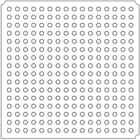
LFXP2-8E-5FTN256I Lattice, LFXP2-8E-5FTN256I Datasheet - Page 167

LFXP2-8E-5FTN256I
Manufacturer Part Number
LFXP2-8E-5FTN256I
Description
FPGA - Field Programmable Gate Array 8K LUTs 201 I/O Inst on DSP 1.2V -5 Spd
Manufacturer
Lattice
Datasheet
1.LFXP2-8E-5FTN256I.pdf
(341 pages)
Specifications of LFXP2-8E-5FTN256I
Number Of Macrocells
8000
Number Of Programmable I/os
201
Data Ram Size
226304
Supply Voltage (max)
1.26 V
Maximum Operating Temperature
+ 100 C
Minimum Operating Temperature
- 40 C
Mounting Style
SMD/SMT
Supply Voltage (min)
1.14 V
Package / Case
FTBGA-256
Number Of Logic Elements/cells
*
Number Of Labs/clbs
*
Total Ram Bits
226304
Number Of I /o
201
Number Of Gates
-
Voltage - Supply
1.14 V ~ 1.26 V
Mounting Type
*
Operating Temperature
-40°C ~ 100°C
Package
256FTBGA
Family Name
LatticeXP2
Device Logic Units
8000
Typical Operating Supply Voltage
1.2 V
Maximum Number Of User I/os
201
Ram Bits
226304
Re-programmability Support
Yes
Lead Free Status / RoHS Status
Lead free / RoHS Compliant
Available stocks
Company
Part Number
Manufacturer
Quantity
Price
Company:
Part Number:
LFXP2-8E-5FTN256I
Manufacturer:
Lattice Semiconductor Corporation
Quantity:
10 000
- Current page: 167 of 341
- Download datasheet (10Mb)
Lattice Semiconductor
Pseudo Dual Port RAM (RAM_DP) – EBR Based
The EBR blocks in LatticeXP2 devices can be configured as Pseudo-Dual Port RAM or RAM_DP. IPexpress allows
users to generate the Verilog-HDL or VHDL along with EDIF netlists for the memory size as per design require-
ments.
IPexpress generates the memory module as shown in Figure 10-15.
Figure 10-15. Pseudo Dual Port Memory Module Generated by IPexpress
The generated module makes use of these EBR blocks or primitives. For memory sizes smaller than an EBR block,
the module will be created in one EBR block. If the specified memory is larger than one EBR block, multiple EBR
blocks can be cascaded in depth or width (as required to create these sizes).
In Pseudo Dual Port RAM mode, the input data and address for the ports are registered at the input of the memory
array. The output data of the memory is optionally registered at the output.
The various ports and their definitions for the Single Port Memory are listed in Table 10-8. The table lists the corre-
sponding ports for the module generated by IPexpress and for the EBR RAM_DP primitive.
Table 10-8. EBR-based Pseudo-Dual Port Memory Port Definitions
Reset (RST) resets only the input and output registers of the RAM. It does not reset the contents of the memory.
Chip Select (CS) is a useful port when multiple cascaded EBR blocks are required by the memory. The CS signal
forms the MSB for the address when multiple EBR blocks are cascaded. Since CS is a 3-bit bus, it can cascade
eight memories easily. However, if the memory size specified by the user requires more than eight EBR blocks, the
ispLEVER software automatically generates the additional address decoding logic, which is implemented in the
PFU external to the EBR blocks.
Generated Module
Port Name in
RdAddress
WrAddress
RdClockEn
WrClockEn
RdClock
WrClock
Reset
Data
WE
—
Q
WrAddress
WrClockEn
EBR Block Primitive
WrClock
Port Name in the
Reset
Data
ADW[x2:0]
ADR[x1:0]
DO[y1:0]
WE
DI[y2:0]
CS[2:0]
CLKW
CLKR
CEW
CER
RST
WE
EBR based Pseudo
Dual Port Memory
RAM_DP
10-17
Read Clock Enable
Write Clock Enable
Read Address
Write Address
Write Enable
Description
Read Clock
Write Clock
Chip Select
Read Data
Write Data
Reset
LatticeXP2 Memory Usage Guide
RdClock
RdClockEn
RdAddress
Q
Rising Clock Edge
Rising Clock Edge
Active State
Active High
Active High
Active High
Active High
—
—
—
—
—
Related parts for LFXP2-8E-5FTN256I
Image
Part Number
Description
Manufacturer
Datasheet
Request
R

Part Number:
Description:
FPGA - Field Programmable Gate Array 8K LUTs 100I/O Inst- on DSP 1.2V -5 Spd
Manufacturer:
Lattice
Datasheet:

Part Number:
Description:
FPGA - Field Programmable Gate Array 8K LUTs 201I/O Inst- on DSP 1.2V -5 Spd
Manufacturer:
Lattice
Datasheet:

Part Number:
Description:
FPGA - Field Programmable Gate Array 8K LUTs 100 I/O Inst on DSP 1.2V -5 Spd
Manufacturer:
Lattice
Datasheet:

Part Number:
Description:
IC, LATTICEXP2 FPGA, 435MHZ, QFP-208
Manufacturer:
LATTICE SEMICONDUCTOR
Datasheet:

Part Number:
Description:
FPGA - Field Programmable Gate Array 8K LUTs 86I/O Inst- on DSP 1.2V -5 Spd
Manufacturer:
Lattice

Part Number:
Description:
FPGA - Field Programmable Gate Array 8K LUTs 201I/O Inst- on DSP 1.2V -7 Spd
Manufacturer:
Lattice
Datasheet:
Part Number:
Description:
FPGA LatticeXP2 Family 8000 Cells Flash Technology 1.2V 144-Pin TQFP
Manufacturer:
LATTICE SEMICONDUCTOR
Datasheet:

Part Number:
Description:
IC DSP 8KLUTS 146I/O 208PQFP
Manufacturer:
Lattice
Datasheet:

Part Number:
Description:
IC DSP 8KLUTS 100I/O 144TQFP
Manufacturer:
Lattice
Datasheet:

Part Number:
Description:
IC DSP 8KLUTS 86I/O 132CSBGA
Manufacturer:
Lattice
Datasheet:

Part Number:
Description:
IC DSP 8KLUTS 86I/O 132CSBGA
Manufacturer:
Lattice
Datasheet:

Part Number:
Description:
IC DSP 8KLUTS 146I/O 208PQFP
Manufacturer:
Lattice
Datasheet:

Part Number:
Description:
IC DSP 8KLUTS 201I/O 256FTBGA
Manufacturer:
Lattice
Datasheet:

Part Number:
Description:
IC FPGA 8KLUTS 86I/O 132-BGA
Manufacturer:
Lattice
Datasheet:

Part Number:
Description:
IC FPGA 8KLUTS 86I/O 132-BGA
Manufacturer:
Lattice
Datasheet:


