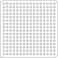
LFXP2-8E-5FTN256I Lattice, LFXP2-8E-5FTN256I Datasheet - Page 218

LFXP2-8E-5FTN256I
Manufacturer Part Number
LFXP2-8E-5FTN256I
Description
FPGA - Field Programmable Gate Array 8K LUTs 201 I/O Inst on DSP 1.2V -5 Spd
Manufacturer
Lattice
Datasheet
1.LFXP2-8E-5FTN256I.pdf
(341 pages)
Specifications of LFXP2-8E-5FTN256I
Number Of Macrocells
8000
Number Of Programmable I/os
201
Data Ram Size
226304
Supply Voltage (max)
1.26 V
Maximum Operating Temperature
+ 100 C
Minimum Operating Temperature
- 40 C
Mounting Style
SMD/SMT
Supply Voltage (min)
1.14 V
Package / Case
FTBGA-256
Number Of Logic Elements/cells
*
Number Of Labs/clbs
*
Total Ram Bits
226304
Number Of I /o
201
Number Of Gates
-
Voltage - Supply
1.14 V ~ 1.26 V
Mounting Type
*
Operating Temperature
-40°C ~ 100°C
Package
256FTBGA
Family Name
LatticeXP2
Device Logic Units
8000
Typical Operating Supply Voltage
1.2 V
Maximum Number Of User I/os
201
Ram Bits
226304
Re-programmability Support
Yes
Lead Free Status / RoHS Status
Lead free / RoHS Compliant
Available stocks
Company
Part Number
Manufacturer
Quantity
Price
Company:
Part Number:
LFXP2-8E-5FTN256I
Manufacturer:
Lattice Semiconductor Corporation
Quantity:
10 000
- Current page: 218 of 341
- Download datasheet (10Mb)
Lattice Semiconductor
Figure 11-18. ODDRMXA Waveform
Note that the DQSXFER is inverted inside the ODDRXMA. This will cause the data coming out of the ODDRXMA
to be -90° in phase with the output of the ODDRXC module.
Memory Read Implementation
LatticeXP2 devices contain a variety of features to simplify implementation of the read portion of a DDR interface:
• DLL compensated DQS delay elements
• DDR input registers
• Automatic DQS to system clock domain transfer circuitry
• Data Valid Module
DLL Compensated DQS Delay Elements
The DQS from the memory is connected to the DQS Delay element. The DQS Delay block receives a 6-bit delay
control from the on-chip DQSDLL. The LatticeXP2 devices support two DQSDLL, one on the left and one on the
right side of the device. The DQSDEL generated by the DQSDLL on the left side is routed to all the DQS blocks on
the left and bottom/top half of the device. The delay generated by the DQSDLL on the right side is distributed to all
the DQS Delay blocks on the right side and the other bottom/top half of the device. These digital delay control sig-
nals are used to delay the DQS from the memory by 90 degrees.
The DQS received from the memory is delayed in each of the DQS Delay blocks and this delay DQS is used to
clock the first set stage DDR input registers.
DQS Transition Detect or Automatic Clock Polarity Select
In a typical DDR memory interface design, the phase relation between the incoming delayed DQS strobe and the
internal system clock (during the READ cycle) is unknown. Prior to the READ operation in DDR memories, DQS is
in tristate (pulled by termination). Coming out of tristate, the DDR memory device drives DQS low in the Preamble
State. The DQS Transition Detect block detects the first DQS rising edge after the Preamble transition and gener-
ates a signal indicating the required polarity for the FPGA system clock (DDRCLKPOL). This signal is used to con-
trol the polarity of the clock to the synchronizing registers.
DQSXFER
Latch C0
Reg B0
Reg A0
ECLK
DA
DB
Q
XX
XX
XX
XX
XX
XX
P0
N0
P0
N0
P0
P1
N1
N0
N0
11-14
P1
N1
P1
P2
N2
N1
N1
LatticeXP2 High-Speed I/O Interface
P2
P2
N2
N3
P3
N2
N2
P3
P3
N3
P4
N4
N3
N3
P4
P4
N4
..
..
Related parts for LFXP2-8E-5FTN256I
Image
Part Number
Description
Manufacturer
Datasheet
Request
R

Part Number:
Description:
FPGA - Field Programmable Gate Array 8K LUTs 100I/O Inst- on DSP 1.2V -5 Spd
Manufacturer:
Lattice
Datasheet:

Part Number:
Description:
FPGA - Field Programmable Gate Array 8K LUTs 201I/O Inst- on DSP 1.2V -5 Spd
Manufacturer:
Lattice
Datasheet:

Part Number:
Description:
FPGA - Field Programmable Gate Array 8K LUTs 100 I/O Inst on DSP 1.2V -5 Spd
Manufacturer:
Lattice
Datasheet:

Part Number:
Description:
IC, LATTICEXP2 FPGA, 435MHZ, QFP-208
Manufacturer:
LATTICE SEMICONDUCTOR
Datasheet:

Part Number:
Description:
FPGA - Field Programmable Gate Array 8K LUTs 86I/O Inst- on DSP 1.2V -5 Spd
Manufacturer:
Lattice

Part Number:
Description:
FPGA - Field Programmable Gate Array 8K LUTs 201I/O Inst- on DSP 1.2V -7 Spd
Manufacturer:
Lattice
Datasheet:
Part Number:
Description:
FPGA LatticeXP2 Family 8000 Cells Flash Technology 1.2V 144-Pin TQFP
Manufacturer:
LATTICE SEMICONDUCTOR
Datasheet:

Part Number:
Description:
IC DSP 8KLUTS 146I/O 208PQFP
Manufacturer:
Lattice
Datasheet:

Part Number:
Description:
IC DSP 8KLUTS 100I/O 144TQFP
Manufacturer:
Lattice
Datasheet:

Part Number:
Description:
IC DSP 8KLUTS 86I/O 132CSBGA
Manufacturer:
Lattice
Datasheet:

Part Number:
Description:
IC DSP 8KLUTS 86I/O 132CSBGA
Manufacturer:
Lattice
Datasheet:

Part Number:
Description:
IC DSP 8KLUTS 146I/O 208PQFP
Manufacturer:
Lattice
Datasheet:

Part Number:
Description:
IC DSP 8KLUTS 201I/O 256FTBGA
Manufacturer:
Lattice
Datasheet:

Part Number:
Description:
IC FPGA 8KLUTS 86I/O 132-BGA
Manufacturer:
Lattice
Datasheet:

Part Number:
Description:
IC FPGA 8KLUTS 86I/O 132-BGA
Manufacturer:
Lattice
Datasheet:


