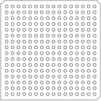
LFXP2-8E-5FTN256I Lattice, LFXP2-8E-5FTN256I Datasheet - Page 124

LFXP2-8E-5FTN256I
Manufacturer Part Number
LFXP2-8E-5FTN256I
Description
FPGA - Field Programmable Gate Array 8K LUTs 201 I/O Inst on DSP 1.2V -5 Spd
Manufacturer
Lattice
Datasheet
1.LFXP2-8E-5FTN256I.pdf
(341 pages)
Specifications of LFXP2-8E-5FTN256I
Number Of Macrocells
8000
Number Of Programmable I/os
201
Data Ram Size
226304
Supply Voltage (max)
1.26 V
Maximum Operating Temperature
+ 100 C
Minimum Operating Temperature
- 40 C
Mounting Style
SMD/SMT
Supply Voltage (min)
1.14 V
Package / Case
FTBGA-256
Number Of Logic Elements/cells
*
Number Of Labs/clbs
*
Total Ram Bits
226304
Number Of I /o
201
Number Of Gates
-
Voltage - Supply
1.14 V ~ 1.26 V
Mounting Type
*
Operating Temperature
-40°C ~ 100°C
Package
256FTBGA
Family Name
LatticeXP2
Device Logic Units
8000
Typical Operating Supply Voltage
1.2 V
Maximum Number Of User I/os
201
Ram Bits
226304
Re-programmability Support
Yes
Lead Free Status / RoHS Status
Lead free / RoHS Compliant
Available stocks
Company
Part Number
Manufacturer
Quantity
Price
Company:
Part Number:
LFXP2-8E-5FTN256I
Manufacturer:
Lattice Semiconductor Corporation
Quantity:
10 000
- Current page: 124 of 341
- Download datasheet (10Mb)
Lattice Semiconductor
Primary Clocks
Each quadrant receives up to eight primary clocks. Two of these clocks provide the Dynamic Clock Selection (DCS)
feature. The six primary clocks without DCS can be specified in the Pre-map Preference Editor as ‘Primary Pure’
and the two DCS clocks as ‘Primary-DCS’.
The sources of primary clocks are:
• PLL outputs
• CLKDIV outputs
• Dedicated clock pins
• Internal nodes
Secondary Clocks
The LatticeXP2 secondary clocks are a flexible region-based clocking resource. Each region can have four inde-
pendent clock inputs. Since the secondary clock is a regional resource, it can cross the primary clock quadrant
boundaries.
There are eight secondary clock muxes per quadrant. Each mux has inputs from four different sources. Three of
these are from internal nodes. The fourth input comes from a primary clock pin. The input sources are not neces-
sarily located in the same quadrant as the mux. This structure enables global use of secondary clocks.
The sources of secondary clocks are:
• Dedicated clock pins
• Clock Divider (CLKDIV) outputs
• Internal nodes
Table 9-2 lists the number of secondary clock regions in LatticeXP2 devices.
Table 9-2. Number of Secondary Clock Regions
Edge Clocks
The LatticeXP2 device has two Edge Clocks (ECLK) per side. These clocks, which have low injection time and
skew, are used to clock I/O registers. Edge clock resources are designed for high speed I/O interfaces with high
fanout capability. Refer to Appendix B for detailed information on ECLK locations and connectivity.
The sources of edge clocks are:
• Left and Right Edge Clocks
• Top and Bottom Edge Clocks
Edge clocks can directly drive the secondary clock resources and general routing resources. Refer to Figure 9-21
for detailed information on edge clock routing.
– Dedicated clock pins
– PLL outputs
– PLL input pins
– Internal nodes
– Dedicated clock pins
– Internal nodes
Number of regions
Parameter
XP2-5
6
9-2
XP2-8
6
XP2-17
6
LatticeXP2 sysCLOCK PLL
XP2-30
Design and Usage Guide
6
XP2-40
8
Related parts for LFXP2-8E-5FTN256I
Image
Part Number
Description
Manufacturer
Datasheet
Request
R

Part Number:
Description:
FPGA - Field Programmable Gate Array 8K LUTs 100I/O Inst- on DSP 1.2V -5 Spd
Manufacturer:
Lattice
Datasheet:

Part Number:
Description:
FPGA - Field Programmable Gate Array 8K LUTs 201I/O Inst- on DSP 1.2V -5 Spd
Manufacturer:
Lattice
Datasheet:

Part Number:
Description:
FPGA - Field Programmable Gate Array 8K LUTs 100 I/O Inst on DSP 1.2V -5 Spd
Manufacturer:
Lattice
Datasheet:

Part Number:
Description:
IC, LATTICEXP2 FPGA, 435MHZ, QFP-208
Manufacturer:
LATTICE SEMICONDUCTOR
Datasheet:

Part Number:
Description:
FPGA - Field Programmable Gate Array 8K LUTs 86I/O Inst- on DSP 1.2V -5 Spd
Manufacturer:
Lattice

Part Number:
Description:
FPGA - Field Programmable Gate Array 8K LUTs 201I/O Inst- on DSP 1.2V -7 Spd
Manufacturer:
Lattice
Datasheet:
Part Number:
Description:
FPGA LatticeXP2 Family 8000 Cells Flash Technology 1.2V 144-Pin TQFP
Manufacturer:
LATTICE SEMICONDUCTOR
Datasheet:

Part Number:
Description:
IC DSP 8KLUTS 146I/O 208PQFP
Manufacturer:
Lattice
Datasheet:

Part Number:
Description:
IC DSP 8KLUTS 100I/O 144TQFP
Manufacturer:
Lattice
Datasheet:

Part Number:
Description:
IC DSP 8KLUTS 86I/O 132CSBGA
Manufacturer:
Lattice
Datasheet:

Part Number:
Description:
IC DSP 8KLUTS 86I/O 132CSBGA
Manufacturer:
Lattice
Datasheet:

Part Number:
Description:
IC DSP 8KLUTS 146I/O 208PQFP
Manufacturer:
Lattice
Datasheet:

Part Number:
Description:
IC DSP 8KLUTS 201I/O 256FTBGA
Manufacturer:
Lattice
Datasheet:

Part Number:
Description:
IC FPGA 8KLUTS 86I/O 132-BGA
Manufacturer:
Lattice
Datasheet:

Part Number:
Description:
IC FPGA 8KLUTS 86I/O 132-BGA
Manufacturer:
Lattice
Datasheet:


