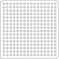
LFXP2-8E-5FTN256I Lattice, LFXP2-8E-5FTN256I Datasheet - Page 207

LFXP2-8E-5FTN256I
Manufacturer Part Number
LFXP2-8E-5FTN256I
Description
FPGA - Field Programmable Gate Array 8K LUTs 201 I/O Inst on DSP 1.2V -5 Spd
Manufacturer
Lattice
Datasheet
1.LFXP2-8E-5FTN256I.pdf
(341 pages)
Specifications of LFXP2-8E-5FTN256I
Number Of Macrocells
8000
Number Of Programmable I/os
201
Data Ram Size
226304
Supply Voltage (max)
1.26 V
Maximum Operating Temperature
+ 100 C
Minimum Operating Temperature
- 40 C
Mounting Style
SMD/SMT
Supply Voltage (min)
1.14 V
Package / Case
FTBGA-256
Number Of Logic Elements/cells
*
Number Of Labs/clbs
*
Total Ram Bits
226304
Number Of I /o
201
Number Of Gates
-
Voltage - Supply
1.14 V ~ 1.26 V
Mounting Type
*
Operating Temperature
-40°C ~ 100°C
Package
256FTBGA
Family Name
LatticeXP2
Device Logic Units
8000
Typical Operating Supply Voltage
1.2 V
Maximum Number Of User I/os
201
Ram Bits
226304
Re-programmability Support
Yes
Lead Free Status / RoHS Status
Lead free / RoHS Compliant
Available stocks
Company
Part Number
Manufacturer
Quantity
Price
Company:
Part Number:
LFXP2-8E-5FTN256I
Manufacturer:
Lattice Semiconductor Corporation
Quantity:
10 000
- Current page: 207 of 341
- Download datasheet (10Mb)
Lattice Semiconductor
Figure 11-4. DQ-DQS During WRITE
Implementing DDR Memory Interfaces with LatticeXP2 Devices
As described in the DDRSDRAM overview section, the DDR SDRAM interfaces rely primarily on the use of a data
strobe signal called DQS for high-speed operation. When reading data from the external memory device, data
coming into the LatticeXP2 device is edge-aligned with respect to the DQS signal. Therefore, the LatticeXP2 device
needs to shift the DQS (a 90-degree phase shift) before using it to sample the read data. When writing to a DDR
SDRAM, the memory controller from the LatticeXP2 device must generate a DQS signal that is center-aligned with
the DQ, the data signals. This is accomplished by ensuring the DQS strobe is 90 degrees ahead relative to DQ
data.
LatticeXP2 devices have dedicated DQS support circuitry for generating the appropriate phase shifting for DQS.
The DQS phase shift circuit uses a frequency reference DLL to generate delay control signals associated with each
of the dedicated DQS pins and is designed to compensate for process, voltage and temperature (PVT) variations.
The frequency reference is provided through one of the global clock pins.
The dedicated DDR support circuit is also designed to provide comfortable and consistent margins for data sam-
pling window.
This section describes how to implement the read and write sections of a DDR memory interface. It also provides
details of the DQ and DQS grouping rules associated with the LatticeXP2 devices.
DQS Grouping
Each DQS group generally consists of at least 10 I/Os (one DQS, eight DQ and one DM) to implement a complete
8-bit DDR memory interface. LatticeXP2 devices support DQS signals on all sides of the device. Each DQS signal
on the top and bottom halves of the device will span across 18 I/Os and on the left and right sides of the device will
span across 16 I/Os. Any 10 of these I/Os spanned by the DQS can be used to implement an 8-bit DDR memory
interface. In addition to the DQS grouping, the user must also assign one reference voltage VREF1 for a given I/O
bank.
Figure 11-5. DQ-DQS Grouping
(at PIN)
(at PIN)
DQS
DQ
*n=18 on bottom banks and n=16 on the left and right side banks.
DQ or DM
(Ninth I/O Pad)
n* I/O PADS
DQS PAD
11-3
LatticeXP2 High-Speed I/O Interface
DQ or DM
Related parts for LFXP2-8E-5FTN256I
Image
Part Number
Description
Manufacturer
Datasheet
Request
R

Part Number:
Description:
FPGA - Field Programmable Gate Array 8K LUTs 100I/O Inst- on DSP 1.2V -5 Spd
Manufacturer:
Lattice
Datasheet:

Part Number:
Description:
FPGA - Field Programmable Gate Array 8K LUTs 201I/O Inst- on DSP 1.2V -5 Spd
Manufacturer:
Lattice
Datasheet:

Part Number:
Description:
FPGA - Field Programmable Gate Array 8K LUTs 100 I/O Inst on DSP 1.2V -5 Spd
Manufacturer:
Lattice
Datasheet:

Part Number:
Description:
IC, LATTICEXP2 FPGA, 435MHZ, QFP-208
Manufacturer:
LATTICE SEMICONDUCTOR
Datasheet:

Part Number:
Description:
FPGA - Field Programmable Gate Array 8K LUTs 86I/O Inst- on DSP 1.2V -5 Spd
Manufacturer:
Lattice

Part Number:
Description:
FPGA - Field Programmable Gate Array 8K LUTs 201I/O Inst- on DSP 1.2V -7 Spd
Manufacturer:
Lattice
Datasheet:
Part Number:
Description:
FPGA LatticeXP2 Family 8000 Cells Flash Technology 1.2V 144-Pin TQFP
Manufacturer:
LATTICE SEMICONDUCTOR
Datasheet:

Part Number:
Description:
IC DSP 8KLUTS 146I/O 208PQFP
Manufacturer:
Lattice
Datasheet:

Part Number:
Description:
IC DSP 8KLUTS 100I/O 144TQFP
Manufacturer:
Lattice
Datasheet:

Part Number:
Description:
IC DSP 8KLUTS 86I/O 132CSBGA
Manufacturer:
Lattice
Datasheet:

Part Number:
Description:
IC DSP 8KLUTS 86I/O 132CSBGA
Manufacturer:
Lattice
Datasheet:

Part Number:
Description:
IC DSP 8KLUTS 146I/O 208PQFP
Manufacturer:
Lattice
Datasheet:

Part Number:
Description:
IC DSP 8KLUTS 201I/O 256FTBGA
Manufacturer:
Lattice
Datasheet:

Part Number:
Description:
IC FPGA 8KLUTS 86I/O 132-BGA
Manufacturer:
Lattice
Datasheet:

Part Number:
Description:
IC FPGA 8KLUTS 86I/O 132-BGA
Manufacturer:
Lattice
Datasheet:


