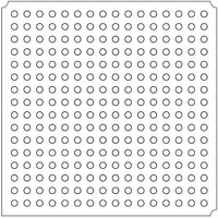
LFXP2-8E-5FTN256I Lattice, LFXP2-8E-5FTN256I Datasheet - Page 220

LFXP2-8E-5FTN256I
Manufacturer Part Number
LFXP2-8E-5FTN256I
Description
FPGA - Field Programmable Gate Array 8K LUTs 201 I/O Inst on DSP 1.2V -5 Spd
Manufacturer
Lattice
Datasheet
1.LFXP2-8E-5FTN256I.pdf
(341 pages)
Specifications of LFXP2-8E-5FTN256I
Number Of Macrocells
8000
Number Of Programmable I/os
201
Data Ram Size
226304
Supply Voltage (max)
1.26 V
Maximum Operating Temperature
+ 100 C
Minimum Operating Temperature
- 40 C
Mounting Style
SMD/SMT
Supply Voltage (min)
1.14 V
Package / Case
FTBGA-256
Number Of Logic Elements/cells
*
Number Of Labs/clbs
*
Total Ram Bits
226304
Number Of I /o
201
Number Of Gates
-
Voltage - Supply
1.14 V ~ 1.26 V
Mounting Type
*
Operating Temperature
-40°C ~ 100°C
Package
256FTBGA
Family Name
LatticeXP2
Device Logic Units
8000
Typical Operating Supply Voltage
1.2 V
Maximum Number Of User I/os
201
Ram Bits
226304
Re-programmability Support
Yes
Lead Free Status / RoHS Status
Lead free / RoHS Compliant
Available stocks
Company
Part Number
Manufacturer
Quantity
Price
Company:
Part Number:
LFXP2-8E-5FTN256I
Manufacturer:
Lattice Semiconductor Corporation
Quantity:
10 000
- Current page: 220 of 341
- Download datasheet (10Mb)
Lattice Semiconductor
Figure 11-20. Software Primitive Implementation for Memory READ (Full Clock Transfer)
Read Timing Waveforms
Figures 11-21 and 11-22 show READ data transfer for half and full clock cycle data transfer based on the results of
the DQS Transition detector logic. This circuitry decides whether or not to invert the phase of FPGA system CLK to
the synchronization registers based on the relative phases of PRMBDET and CLK.
• Case 1: If the FPGA clock is low on the first PRMBDET transition, then DDRCLKPOL is low and no inversion is
• Case 2: If the FPGA clock is high on the first PRMBDET, then DDRCLKPOL is high and the FPGA clock (CLK)
Figure 11-21 illustrates the DDR data timing using half clock transfer mode at different stages of the IDDRMX1A
registers. The first stage of the register captures data on the positive edge as shown by signal A and the negative
edge as shown by signal B. Data stream A goes through an additional half clock cycle transfer shown by signal C.
Phase-aligned data streams B and C are presented to the next stage registers clocked by the FPGA clock.
Figure 11-22 illustrates the DDR data timing using full clock transfer mode at different stages of IDDRMFX1A regis-
ters. In addition to the first two register stages in the half clock mode, the full clock transfer mode has an additional
stage register clocked by the FPGA clock. In this case, D and E are the data streams after the second register
stage presented to the final stage of registers clocked by the FPGA clock.
dqs
dq
required.
needs to be inverted before it is used for synchronization.
uddcntl
reset
read
xclk
clk
ce
RST
UDDCNTL
DQSI
CLK
READ
XCLK
DQSBUFC
DQSDEL
DQSDEL
DQSDLL
6
DDRCLKPOL
DATAVALID
PRMBDET
DQSXFER
DQSO
DQSC
LOCK
11-16
LatticeXP2 High-Speed I/O Interface
ECLK
DDRCLKPOL
RST
CE
CLK1
CLK2
D
IDDRMFX1A
QA
QB
dqsc
prmbdet
dqsxfer
datavalid
lock
datain_p
datain_n
Related parts for LFXP2-8E-5FTN256I
Image
Part Number
Description
Manufacturer
Datasheet
Request
R

Part Number:
Description:
FPGA - Field Programmable Gate Array 8K LUTs 100I/O Inst- on DSP 1.2V -5 Spd
Manufacturer:
Lattice
Datasheet:

Part Number:
Description:
FPGA - Field Programmable Gate Array 8K LUTs 201I/O Inst- on DSP 1.2V -5 Spd
Manufacturer:
Lattice
Datasheet:

Part Number:
Description:
FPGA - Field Programmable Gate Array 8K LUTs 100 I/O Inst on DSP 1.2V -5 Spd
Manufacturer:
Lattice
Datasheet:

Part Number:
Description:
IC, LATTICEXP2 FPGA, 435MHZ, QFP-208
Manufacturer:
LATTICE SEMICONDUCTOR
Datasheet:

Part Number:
Description:
FPGA - Field Programmable Gate Array 8K LUTs 86I/O Inst- on DSP 1.2V -5 Spd
Manufacturer:
Lattice

Part Number:
Description:
FPGA - Field Programmable Gate Array 8K LUTs 201I/O Inst- on DSP 1.2V -7 Spd
Manufacturer:
Lattice
Datasheet:
Part Number:
Description:
FPGA LatticeXP2 Family 8000 Cells Flash Technology 1.2V 144-Pin TQFP
Manufacturer:
LATTICE SEMICONDUCTOR
Datasheet:

Part Number:
Description:
IC DSP 8KLUTS 146I/O 208PQFP
Manufacturer:
Lattice
Datasheet:

Part Number:
Description:
IC DSP 8KLUTS 100I/O 144TQFP
Manufacturer:
Lattice
Datasheet:

Part Number:
Description:
IC DSP 8KLUTS 86I/O 132CSBGA
Manufacturer:
Lattice
Datasheet:

Part Number:
Description:
IC DSP 8KLUTS 86I/O 132CSBGA
Manufacturer:
Lattice
Datasheet:

Part Number:
Description:
IC DSP 8KLUTS 146I/O 208PQFP
Manufacturer:
Lattice
Datasheet:

Part Number:
Description:
IC DSP 8KLUTS 201I/O 256FTBGA
Manufacturer:
Lattice
Datasheet:

Part Number:
Description:
IC FPGA 8KLUTS 86I/O 132-BGA
Manufacturer:
Lattice
Datasheet:

Part Number:
Description:
IC FPGA 8KLUTS 86I/O 132-BGA
Manufacturer:
Lattice
Datasheet:


