YLCDRSK2378 Renesas Electronics America, YLCDRSK2378 Datasheet - Page 286
YLCDRSK2378
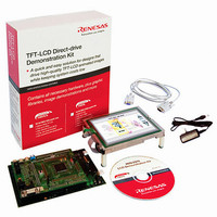
Manufacturer Part Number
YLCDRSK2378
Description
KIT DEV EVAL H8S/2378 LCD
Manufacturer
Renesas Electronics America
Series
H8®r
Datasheet
1.YR0K42378FC000BA.pdf
(1208 pages)
Specifications of YLCDRSK2378
Main Purpose
Displays, LCD Controller
Embedded
Yes, MCU, 16-Bit
Utilized Ic / Part
YLCDRSK2378
Primary Attributes
5.7" QVGA, Touch Screen
Secondary Attributes
Source Code on CD, Debugging Requires Emulator Cable E10A USB/JTAG
Lead Free Status / RoHS Status
Lead free / RoHS Compliant


Section 6 Bus Controller (BSC)
6.7.3
If the ABW2 bit in ABWCR corresponding to an area designated as continuous synchronous
DRAM space is set to 1, area 2 to 5 are designated as 8-bit continuous synchronous DRAM space;
if the bit is cleared to 0, the areas are designated as 16-bit continuous synchronous DRAM space.
In 16-bit continuous synchronous DRAM space, ×16-bit configuration synchronous DRAM can be
connected directly.
In 8-bit continuous synchronous DRAM space the upper half of the data bus, D15 to D8, is
enabled, while in 16-bit continuous synchronous DRAM space both the upper and lower halves of
the data bus, D15 to D0, are enabled.
Access sizes and data alignment are the same as for the basic bus interface: see section 6.5.1, Data
Size and Data Alignment.
6.7.4
Table 6.9 shows pins used for the synchronous DRAM interface and their functions. To enable the
synchronous DRAM interface, fix the DCTL pin to 1. Do not vary the DCTL pin during operation.
Since the CS2 to CS4 pins are in the input state after a reset, set DDR to 1 when RAS, CAS, and
WE signals are output. For details, see section 10, I/O Ports. Set the OEE bit of the DRAMCR
register to 1 when the CKE signal is output.
Rev.7.00 Mar. 18, 2009 page 218 of 1136
REJ09B0109-0700
Data Bus
Pins Used for Synchronous DRAM Interface
Related parts for YLCDRSK2378
Image
Part Number
Description
Manufacturer
Datasheet
Request
R

Part Number:
Description:
KIT STARTER FOR M16C/29
Manufacturer:
Renesas Electronics America
Datasheet:

Part Number:
Description:
KIT STARTER FOR R8C/2D
Manufacturer:
Renesas Electronics America
Datasheet:

Part Number:
Description:
R0K33062P STARTER KIT
Manufacturer:
Renesas Electronics America
Datasheet:

Part Number:
Description:
KIT STARTER FOR R8C/23 E8A
Manufacturer:
Renesas Electronics America
Datasheet:

Part Number:
Description:
KIT STARTER FOR R8C/25
Manufacturer:
Renesas Electronics America
Datasheet:

Part Number:
Description:
KIT STARTER H8S2456 SHARPE DSPLY
Manufacturer:
Renesas Electronics America
Datasheet:

Part Number:
Description:
KIT STARTER FOR R8C38C
Manufacturer:
Renesas Electronics America
Datasheet:

Part Number:
Description:
KIT STARTER FOR R8C35C
Manufacturer:
Renesas Electronics America
Datasheet:

Part Number:
Description:
KIT STARTER FOR R8CL3AC+LCD APPS
Manufacturer:
Renesas Electronics America
Datasheet:
Part Number:
Description:
KIT STARTER FOR RX610
Manufacturer:
Renesas Electronics America
Datasheet:

Part Number:
Description:
KIT STARTER FOR R32C/118
Manufacturer:
Renesas Electronics America
Datasheet:

Part Number:
Description:
KIT DEV RSK-R8C/26-29
Manufacturer:
Renesas Electronics America
Datasheet:

Part Number:
Description:
KIT STARTER FOR SH7124
Manufacturer:
Renesas Electronics America
Datasheet:

Part Number:
Description:
KIT STARTER FOR H8SX/1622
Manufacturer:
Renesas Electronics America
Datasheet:

Part Number:
Description:
KIT DEV FOR SH7203
Manufacturer:
Renesas Electronics America
Datasheet: