YLCDRSK2378 Renesas Electronics America, YLCDRSK2378 Datasheet - Page 537
YLCDRSK2378
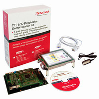
Manufacturer Part Number
YLCDRSK2378
Description
KIT DEV EVAL H8S/2378 LCD
Manufacturer
Renesas Electronics America
Series
H8®r
Datasheet
1.YR0K42378FC000BA.pdf
(1208 pages)
Specifications of YLCDRSK2378
Main Purpose
Displays, LCD Controller
Embedded
Yes, MCU, 16-Bit
Utilized Ic / Part
YLCDRSK2378
Primary Attributes
5.7" QVGA, Touch Screen
Secondary Attributes
Source Code on CD, Debugging Requires Emulator Cable E10A USB/JTAG
Lead Free Status / RoHS Status
Lead free / RoHS Compliant


• P12/PO10/TIOCC0/TCLKA
TPU channel 0
settings
P12DDR
NDER10
Pin function
TPU channel 0
settings
MD3 to MD0
IOC3 to IOC0
CCLR2, CCLR0
Output function
Legend:
×: Don’t care
Notes: 1. TIOCC0 input when MD3 to MD0 = B'0000 and IOC3 to IOC0 = B'10××.
The pin function is switched as shown below according to the combination of the TPU channel
0 settings (by bits MD3 to MD0 in TMDR_0, bits IOC3 to IOC0 in TIORL_0, and bits CCLR2
to CCLR0 in TCR_0), bits TPSC2 to TPSC0 in TCR_0 to TCR_5, bit NDER10 in NDERH,
and bit P12DDR.
2. TCLKA input when the setting for any of TCR_0 to TCR_5 is TPSC2 to TPSC0 = B'100.
3. TIOCD0 output disabled.
TCLKA input when phase counting mode is set for channels 1 and 5.
Output disabled and settings (2) effective when BFA = 1 or BFB = 1 in TMDR_0.
TIOCC0 output
(1) in table
B'0000
B'0100
B'1×××
below
(2)
⎯
⎯
⎯
⎯
B'0000
B'0001 to
B'0101 to
compare
B'0011
B'0111
Output
output
(1)
⎯
P12 input
⎯
0
B'001×
B'××00
(2)
⎯
⎯
TCLKA input *
Rev.7.00 Mar. 18, 2009 page 469 of 1136
(2) in table below
TIOCC0 input *
than B'××00
P12 output
PWM *
mode 1
B'0010
output
Other
(1)
⎯
2
1
0
3
PWM mode
1
2 output
Other
B'101
than
Other than B'××00
Section 10 I/O Ports
(1)
REJ09B0109-0700
PO10 output
B''0011
1
1
B'101
(2)
⎯
Related parts for YLCDRSK2378
Image
Part Number
Description
Manufacturer
Datasheet
Request
R

Part Number:
Description:
KIT STARTER FOR M16C/29
Manufacturer:
Renesas Electronics America
Datasheet:

Part Number:
Description:
KIT STARTER FOR R8C/2D
Manufacturer:
Renesas Electronics America
Datasheet:

Part Number:
Description:
R0K33062P STARTER KIT
Manufacturer:
Renesas Electronics America
Datasheet:

Part Number:
Description:
KIT STARTER FOR R8C/23 E8A
Manufacturer:
Renesas Electronics America
Datasheet:

Part Number:
Description:
KIT STARTER FOR R8C/25
Manufacturer:
Renesas Electronics America
Datasheet:

Part Number:
Description:
KIT STARTER H8S2456 SHARPE DSPLY
Manufacturer:
Renesas Electronics America
Datasheet:

Part Number:
Description:
KIT STARTER FOR R8C38C
Manufacturer:
Renesas Electronics America
Datasheet:

Part Number:
Description:
KIT STARTER FOR R8C35C
Manufacturer:
Renesas Electronics America
Datasheet:

Part Number:
Description:
KIT STARTER FOR R8CL3AC+LCD APPS
Manufacturer:
Renesas Electronics America
Datasheet:
Part Number:
Description:
KIT STARTER FOR RX610
Manufacturer:
Renesas Electronics America
Datasheet:

Part Number:
Description:
KIT STARTER FOR R32C/118
Manufacturer:
Renesas Electronics America
Datasheet:

Part Number:
Description:
KIT DEV RSK-R8C/26-29
Manufacturer:
Renesas Electronics America
Datasheet:

Part Number:
Description:
KIT STARTER FOR SH7124
Manufacturer:
Renesas Electronics America
Datasheet:

Part Number:
Description:
KIT STARTER FOR H8SX/1622
Manufacturer:
Renesas Electronics America
Datasheet:

Part Number:
Description:
KIT DEV FOR SH7203
Manufacturer:
Renesas Electronics America
Datasheet: