YLCDRSK2378 Renesas Electronics America, YLCDRSK2378 Datasheet - Page 54
YLCDRSK2378
Manufacturer Part Number
YLCDRSK2378
Description
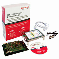
KIT DEV EVAL H8S/2378 LCD
Manufacturer
Renesas Electronics America
Series
H8®r
Datasheet
1.YR0K42378FC000BA.pdf
(1208 pages)
Specifications of YLCDRSK2378
Main Purpose
Displays, LCD Controller
Embedded
Yes, MCU, 16-Bit
Utilized Ic / Part
YLCDRSK2378
Primary Attributes
5.7" QVGA, Touch Screen
Secondary Attributes
Source Code on CD, Debugging Requires Emulator Cable E10A USB/JTAG
Lead Free Status / RoHS Status
Lead free / RoHS Compliant


Figure 11.52 Contention between Overflow and Counter Clearing ............................................. 627
Figure 11.53 Contention between TCNT Write and Overflow..................................................... 628
Section 12 Programmable Pulse Generator (PPG) ............................................ 631
Figure 12.1 Block Diagram of PPG............................................................................................ 632
Figure 12.2 Overview Diagram of PPG...................................................................................... 641
Figure 12.3 Timing of Transfer and Output of NDR Contents (Example) ................................. 642
Figure 12.4 Setup Procedure for Normal Pulse Output (Example) ............................................ 643
Figure 12.5 Normal Pulse Output Example (Five-Phase Pulse Output) ..................................... 644
Figure 12.6 Non-Overlapping Pulse Output ............................................................................... 645
Figure 12.7 Non-Overlapping Operation and NDR Write Timing ............................................. 646
Figure 12.8 Setup Procedure for Non-Overlapping Pulse Output (Example)............................. 647
Figure 12.9 Non-Overlapping Pulse Output Example (Four-Phase Complementary)................ 648
Figure 12.10 Inverted Pulse Output (Example) ............................................................................ 650
Figure 12.11 Pulse Output Triggered by Input Capture (Example).............................................. 651
Section 13 8-Bit Timers (TMR) ........................................................................ 653
Figure 13.1 Block Diagram of 8-Bit Timer Module................................................................... 654
Figure 13.2 Example of Pulse Output......................................................................................... 663
Figure 13.3 Count Timing for Internal Clock Input.................................................................... 664
Figure 13.4 Count Timing for External Clock Input .................................................................. 664
Figure 13.5 Timing of CMF Setting ........................................................................................... 665
Figure 13.6 Timing of Timer Output .......................................................................................... 666
Figure 13.7 Timing of Compare Match Clear ............................................................................ 666
Figure 13.8 Timing of Clearance by External Reset................................................................... 667
Figure 13.9 Timing of OVF Setting............................................................................................ 667
Figure 13.10 Contention between TCNT Write and Clear ........................................................... 670
Figure 13.11 Contention between TCNT Write and Increment.................................................... 671
Figure 13.12 Contention between TCOR Write and Compare Match.......................................... 672
Section 14 Watchdog Timer (WDT) ................................................................. 677
Figure 14.1 Block Diagram of WDT .......................................................................................... 678
Figure 14.2 Operation in Watchdog Timer Mode ...................................................................... 683
Figure 14.3 Operation in Interval Timer Mode .......................................................................... 684
Figure 14.4 Writing to TCNT, TCSR, and RSTCSR.................................................................. 685
Figure 14.5 Contention between TCNT Write and Increment.................................................... 686
Figure 14.6 Circuit for System Reset by WDTOVF Signal (Example)...................................... 687
Section 15 Serial Communication Interface (SCI, IrDA).................................. 689
Figure 15.1 Block Diagram of SCI............................................................................................. 691
Rev.7.00 Mar. 18, 2009 page lii of lxvi
REJ09B0109-0700
Related parts for YLCDRSK2378
Image
Part Number
Description
Manufacturer
Datasheet
Request
R

Part Number:
Description:
KIT STARTER FOR M16C/29
Manufacturer:
Renesas Electronics America
Datasheet:

Part Number:
Description:
KIT STARTER FOR R8C/2D
Manufacturer:
Renesas Electronics America
Datasheet:

Part Number:
Description:
R0K33062P STARTER KIT
Manufacturer:
Renesas Electronics America
Datasheet:

Part Number:
Description:
KIT STARTER FOR R8C/23 E8A
Manufacturer:
Renesas Electronics America
Datasheet:

Part Number:
Description:
KIT STARTER FOR R8C/25
Manufacturer:
Renesas Electronics America
Datasheet:

Part Number:
Description:
KIT STARTER H8S2456 SHARPE DSPLY
Manufacturer:
Renesas Electronics America
Datasheet:

Part Number:
Description:
KIT STARTER FOR R8C38C
Manufacturer:
Renesas Electronics America
Datasheet:

Part Number:
Description:
KIT STARTER FOR R8C35C
Manufacturer:
Renesas Electronics America
Datasheet:

Part Number:
Description:
KIT STARTER FOR R8CL3AC+LCD APPS
Manufacturer:
Renesas Electronics America
Datasheet:
Part Number:
Description:
KIT STARTER FOR RX610
Manufacturer:
Renesas Electronics America
Datasheet:

Part Number:
Description:
KIT STARTER FOR R32C/118
Manufacturer:
Renesas Electronics America
Datasheet:

Part Number:
Description:
KIT DEV RSK-R8C/26-29
Manufacturer:
Renesas Electronics America
Datasheet:

Part Number:
Description:
KIT STARTER FOR SH7124
Manufacturer:
Renesas Electronics America
Datasheet:

Part Number:
Description:
KIT STARTER FOR H8SX/1622
Manufacturer:
Renesas Electronics America
Datasheet:

Part Number:
Description:
KIT DEV FOR SH7203
Manufacturer:
Renesas Electronics America
Datasheet: