YLCDRSK2378 Renesas Electronics America, YLCDRSK2378 Datasheet - Page 346
YLCDRSK2378
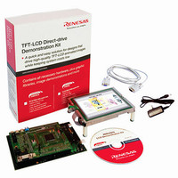
Manufacturer Part Number
YLCDRSK2378
Description
KIT DEV EVAL H8S/2378 LCD
Manufacturer
Renesas Electronics America
Series
H8®r
Datasheet
1.YR0K42378FC000BA.pdf
(1208 pages)
Specifications of YLCDRSK2378
Main Purpose
Displays, LCD Controller
Embedded
Yes, MCU, 16-Bit
Utilized Ic / Part
YLCDRSK2378
Primary Attributes
5.7" QVGA, Touch Screen
Secondary Attributes
Source Code on CD, Debugging Requires Emulator Cable E10A USB/JTAG
Lead Free Status / RoHS Status
Lead free / RoHS Compliant


Section 6 Bus Controller (BSC)
6.14.4
When the BREQOE bit is set to 1 and the BREQO signal is output, BREQO may go low before
the BACK signal.
This will occur if the next external access request or CBR refresh request occurs while internal bus
arbitration is in progress after the chip samples a low level of BREQ.
6.14.5
Setting of Synchronous DRAM Interface: The DCTL pin must be fixed to 1 to enable the
synchronous DRAM interface. Do not change the DCTL pin during operation.
Connection Clock: Be sure to set the clock to be connected to the synchronous DRAM to
SDRAMφ.
WAIT Pin: In the continuous synchronous DRAM space, insertion of the wait state by the WAIT
pin is disabled regardless of the setting of the WAITE bit in BCR.
Bank Control: This LSI cannot carry out the bank control of the synchronous DRAM. All banks
are selected.
Burst Access: The burst read/burst write mode of the synchronous DRAM is not supported.
When setting the mode register of the synchronous DRAM, set to the burst read/single write and
set the burst length to 1.
CAS Latency: When connecting a synchronous DRAM having CAS latency of 1, set the BE bit
to 0 in the DRAMCR.
Note: The synchronous DRAM interface is not supported by the H8S/2378 Group.
Rev.7.00 Mar. 18, 2009 page 278 of 1136
REJ09B0109-0700
BREQO Output Timing
Notes on Usage of the Synchronous DRAM
Related parts for YLCDRSK2378
Image
Part Number
Description
Manufacturer
Datasheet
Request
R

Part Number:
Description:
KIT STARTER FOR M16C/29
Manufacturer:
Renesas Electronics America
Datasheet:

Part Number:
Description:
KIT STARTER FOR R8C/2D
Manufacturer:
Renesas Electronics America
Datasheet:

Part Number:
Description:
R0K33062P STARTER KIT
Manufacturer:
Renesas Electronics America
Datasheet:

Part Number:
Description:
KIT STARTER FOR R8C/23 E8A
Manufacturer:
Renesas Electronics America
Datasheet:

Part Number:
Description:
KIT STARTER FOR R8C/25
Manufacturer:
Renesas Electronics America
Datasheet:

Part Number:
Description:
KIT STARTER H8S2456 SHARPE DSPLY
Manufacturer:
Renesas Electronics America
Datasheet:

Part Number:
Description:
KIT STARTER FOR R8C38C
Manufacturer:
Renesas Electronics America
Datasheet:

Part Number:
Description:
KIT STARTER FOR R8C35C
Manufacturer:
Renesas Electronics America
Datasheet:

Part Number:
Description:
KIT STARTER FOR R8CL3AC+LCD APPS
Manufacturer:
Renesas Electronics America
Datasheet:
Part Number:
Description:
KIT STARTER FOR RX610
Manufacturer:
Renesas Electronics America
Datasheet:

Part Number:
Description:
KIT STARTER FOR R32C/118
Manufacturer:
Renesas Electronics America
Datasheet:

Part Number:
Description:
KIT DEV RSK-R8C/26-29
Manufacturer:
Renesas Electronics America
Datasheet:

Part Number:
Description:
KIT STARTER FOR SH7124
Manufacturer:
Renesas Electronics America
Datasheet:

Part Number:
Description:
KIT STARTER FOR H8SX/1622
Manufacturer:
Renesas Electronics America
Datasheet:

Part Number:
Description:
KIT DEV FOR SH7203
Manufacturer:
Renesas Electronics America
Datasheet: