YLCDRSK2378 Renesas Electronics America, YLCDRSK2378 Datasheet - Page 307
YLCDRSK2378
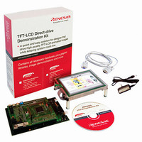
Manufacturer Part Number
YLCDRSK2378
Description
KIT DEV EVAL H8S/2378 LCD
Manufacturer
Renesas Electronics America
Series
H8®r
Datasheet
1.YR0K42378FC000BA.pdf
(1208 pages)
Specifications of YLCDRSK2378
Main Purpose
Displays, LCD Controller
Embedded
Yes, MCU, 16-Bit
Utilized Ic / Part
YLCDRSK2378
Primary Attributes
5.7" QVGA, Touch Screen
Secondary Attributes
Source Code on CD, Debugging Requires Emulator Cable E10A USB/JTAG
Lead Free Status / RoHS Status
Lead free / RoHS Compliant


Refreshing and All-Module-Clocks-Stopped Mode: In this LSI, if the ACSE bit is set to 1 in
MSTPCRH, and then a SLEEP instruction is executed with the setting for all peripheral module
clocks to be stopped (MSTPCR = H'FFFF, EXMSTPCR = H'FFFF) or for operation of the 8-bit
timer module alone (MSTPCR = H'FFFE, EXMSTPCR = H'FFFF), and a transition is made to the
sleep state, the all-module-clocks-stopped mode is entered, in which the bus controller and I/O
port clocks are also stopped.
As the bus controller clock is also stopped in this mode, auto refreshing is not executed. If
synchronous DRAM is connected to the external address space and DRAM data is to be retained
in sleep mode, the ACSE bit must be cleared to 0 in MSTPCR.
Software Standby: When a transition is made to normal software standby, the PALL command is
not output. If synchronous DRAM is connected and DRAM data is to be retained in software
standby, self-refreshing must be set.
DQMU, DQML
Precharge-sel
Address bus
Figure 6.58 Example of Timing when Precharge Time after Self-Refreshing Is Extended
SDRAM
Data bus
CKE
RAS
CAS
WE
φ
φ
by 2 States (TPCS2 to TPCS0 = H'2, TPC1 = 0, TPC0 = 0, CAS Latency 2)
Software
standby
NOP
T
Rc2
T
Rp1
T
Rp2
Column address
Rev.7.00 Mar. 18, 2009 page 239 of 1136
PALL
T
p
Continuous synchronous DRAM space write
Row address
Row address
ACTV
Section 6 Bus Controller (BSC)
T
r
T
NOP
c1
REJ09B0109-0700
Column address
NOP
T
cl
NOP
T
c2
Related parts for YLCDRSK2378
Image
Part Number
Description
Manufacturer
Datasheet
Request
R

Part Number:
Description:
KIT STARTER FOR M16C/29
Manufacturer:
Renesas Electronics America
Datasheet:

Part Number:
Description:
KIT STARTER FOR R8C/2D
Manufacturer:
Renesas Electronics America
Datasheet:

Part Number:
Description:
R0K33062P STARTER KIT
Manufacturer:
Renesas Electronics America
Datasheet:

Part Number:
Description:
KIT STARTER FOR R8C/23 E8A
Manufacturer:
Renesas Electronics America
Datasheet:

Part Number:
Description:
KIT STARTER FOR R8C/25
Manufacturer:
Renesas Electronics America
Datasheet:

Part Number:
Description:
KIT STARTER H8S2456 SHARPE DSPLY
Manufacturer:
Renesas Electronics America
Datasheet:

Part Number:
Description:
KIT STARTER FOR R8C38C
Manufacturer:
Renesas Electronics America
Datasheet:

Part Number:
Description:
KIT STARTER FOR R8C35C
Manufacturer:
Renesas Electronics America
Datasheet:

Part Number:
Description:
KIT STARTER FOR R8CL3AC+LCD APPS
Manufacturer:
Renesas Electronics America
Datasheet:
Part Number:
Description:
KIT STARTER FOR RX610
Manufacturer:
Renesas Electronics America
Datasheet:

Part Number:
Description:
KIT STARTER FOR R32C/118
Manufacturer:
Renesas Electronics America
Datasheet:

Part Number:
Description:
KIT DEV RSK-R8C/26-29
Manufacturer:
Renesas Electronics America
Datasheet:

Part Number:
Description:
KIT STARTER FOR SH7124
Manufacturer:
Renesas Electronics America
Datasheet:

Part Number:
Description:
KIT STARTER FOR H8SX/1622
Manufacturer:
Renesas Electronics America
Datasheet:

Part Number:
Description:
KIT DEV FOR SH7203
Manufacturer:
Renesas Electronics America
Datasheet: