YLCDRSK2378 Renesas Electronics America, YLCDRSK2378 Datasheet - Page 881
YLCDRSK2378
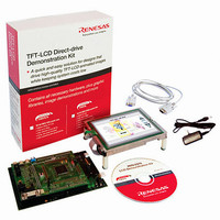
Manufacturer Part Number
YLCDRSK2378
Description
KIT DEV EVAL H8S/2378 LCD
Manufacturer
Renesas Electronics America
Series
H8®r
Datasheet
1.YR0K42378FC000BA.pdf
(1208 pages)
Specifications of YLCDRSK2378
Main Purpose
Displays, LCD Controller
Embedded
Yes, MCU, 16-Bit
Utilized Ic / Part
YLCDRSK2378
Primary Attributes
5.7" QVGA, Touch Screen
Secondary Attributes
Source Code on CD, Debugging Requires Emulator Cable E10A USB/JTAG
Lead Free Status / RoHS Status
Lead free / RoHS Compliant


3. When conversion of all the selected channels is completed, the ADF bit in ADCSR is set to 1.
4. The ADST bit is not cleared automatically, and steps [2] to [3] are repeated as long as the
17.4.3
The A/D converter has a built-in sample-and-hold circuit. The A/D converter samples the analog
input when A/D conversion start delay time (t
conversion. Figure 17.2 shows the A/D conversion timing. Table 17.3 indicates the A/D
conversion time.
As indicated in figure 17.2, the A/D conversion time (t
time (t
total conversion time therefore varies within the ranges indicated in tables 17.3.
In scan mode, the values given in tables 17.3 apply to the first conversion time. The values given
in tables 17.4 apply to the second and subsequent conversions.
If the ADIE bit is set to 1 at this time, an ADI interrupt is requested. Conversion of the first
channel in the group starts again.
ADST bit remains set to 1. When the ADST bit is cleared to 0, A/D conversion stops and the
A/D converter enters wait state. If the ADST bit is later set to 1, A/D conversion starts again
from the first channel in the group.
SPL
). The length of t
Input Sampling and A/D Conversion Time
D
varies depending on the timing of the write access to ADCSR. The
D
) passes after the ADST bit is set to 1, then starts
CONV
Rev.7.00 Mar. 18, 2009 page 813 of 1136
) includes t
D
Section 17 A/D Converter
and the input sampling
REJ09B0109-0700
Related parts for YLCDRSK2378
Image
Part Number
Description
Manufacturer
Datasheet
Request
R

Part Number:
Description:
KIT STARTER FOR M16C/29
Manufacturer:
Renesas Electronics America
Datasheet:

Part Number:
Description:
KIT STARTER FOR R8C/2D
Manufacturer:
Renesas Electronics America
Datasheet:

Part Number:
Description:
R0K33062P STARTER KIT
Manufacturer:
Renesas Electronics America
Datasheet:

Part Number:
Description:
KIT STARTER FOR R8C/23 E8A
Manufacturer:
Renesas Electronics America
Datasheet:

Part Number:
Description:
KIT STARTER FOR R8C/25
Manufacturer:
Renesas Electronics America
Datasheet:

Part Number:
Description:
KIT STARTER H8S2456 SHARPE DSPLY
Manufacturer:
Renesas Electronics America
Datasheet:

Part Number:
Description:
KIT STARTER FOR R8C38C
Manufacturer:
Renesas Electronics America
Datasheet:

Part Number:
Description:
KIT STARTER FOR R8C35C
Manufacturer:
Renesas Electronics America
Datasheet:

Part Number:
Description:
KIT STARTER FOR R8CL3AC+LCD APPS
Manufacturer:
Renesas Electronics America
Datasheet:
Part Number:
Description:
KIT STARTER FOR RX610
Manufacturer:
Renesas Electronics America
Datasheet:

Part Number:
Description:
KIT STARTER FOR R32C/118
Manufacturer:
Renesas Electronics America
Datasheet:

Part Number:
Description:
KIT DEV RSK-R8C/26-29
Manufacturer:
Renesas Electronics America
Datasheet:

Part Number:
Description:
KIT STARTER FOR SH7124
Manufacturer:
Renesas Electronics America
Datasheet:

Part Number:
Description:
KIT STARTER FOR H8SX/1622
Manufacturer:
Renesas Electronics America
Datasheet:

Part Number:
Description:
KIT DEV FOR SH7203
Manufacturer:
Renesas Electronics America
Datasheet: