YLCDRSK2378 Renesas Electronics America, YLCDRSK2378 Datasheet - Page 47
YLCDRSK2378
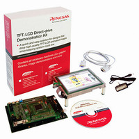
Manufacturer Part Number
YLCDRSK2378
Description
KIT DEV EVAL H8S/2378 LCD
Manufacturer
Renesas Electronics America
Series
H8®r
Datasheet
1.YR0K42378FC000BA.pdf
(1208 pages)
Specifications of YLCDRSK2378
Main Purpose
Displays, LCD Controller
Embedded
Yes, MCU, 16-Bit
Utilized Ic / Part
YLCDRSK2378
Primary Attributes
5.7" QVGA, Touch Screen
Secondary Attributes
Source Code on CD, Debugging Requires Emulator Cable E10A USB/JTAG
Lead Free Status / RoHS Status
Lead free / RoHS Compliant


Figure 6.16 Bus Timing for 16-Bit, 3-State Access Space (Odd Address Byte Access) ............ 185
Figure 6.17 Bus Timing for 16-Bit, 3-State Access Space (Word Access) ................................ 186
Figure 6.18 Example of Wait State Insertion Timing................................................................. 188
Figure 6.19 Example of Read Strobe Timing ............................................................................. 189
Figure 6.20 Example of Timing when Chip Select Assertion Period Is Extended ..................... 190
Figure 6.21 DRAM Basic Access Timing (RAST = 0, CAST = 0)............................................ 194
Figure 6.22 Example of Access Timing with 3-State Column Address Output Cycle
Figure 6.23 Example of Access Timing when RAS Signal Goes Low from Beginning
Figure 6.24 Example of Timing with One Row Address Output Maintenance State
Figure 6.25 Example of Timing with Two-State Precharge Cycle (RAST = 0, CAST = 0)....... 198
Figure 6.26 Example of Wait State Insertion Timing (2-State Column Address Output) .......... 200
Figure 6.27 Example of Wait State Insertion Timing (3-State Column Address Output) .......... 201
Figure 6.28 2-CAS Control Timing (Upper Byte Write Access: RAST = 0, CAST = 0).......... 202
Figure 6.29 Example of 2-CAS DRAM Connection .................................................................. 203
Figure 6.30 Operation Timing in Fast Page Mode (RAST = 0, CAST = 0) ............................... 204
Figure 6.31 Operation Timing in Fast Page Mode (RAST = 0, CAST = 1) ............................... 205
Figure 6.32 Example of Operation Timing in RAS Down Mode (RAST = 0, CAST = 0)......... 206
Figure 6.33 Example of Operation Timing in RAS Up Mode (RAST = 0, CAST = 0).............. 207
Figure 6.34 RTCNT Operation................................................................................................... 208
Figure 6.35 Compare Match Timing .......................................................................................... 209
Figure 6.36 CBR Refresh Timing............................................................................................... 209
Figure 6.37 CBR Refresh Timing (RCW1 = 0, RCW0 = 1, RLW1 = 0, RLW0 = 0)................. 210
Figure 6.38 Example of CBR Refresh Timing (CBRM = 1) ...................................................... 211
Figure 6.39 Self-Refresh Timing ................................................................................................ 212
Figure 6.40 Example of Timing when Precharge Time after Self-Refreshing Is Extended
Figure 6.41 Example of DACK/EDACK Output Timing when DDS = 1 or EDDS = 1
Figure 6.42 Example of DACK/EDACK Output Timing when DDS = 0 or EDDS = 0
Figure 6.43 Relationship between φ and SDRAMφ (when PLL Frequency Multiplication
Figure 6.44 Basic Access Timing of Synchronous DRAM (CAS Latency 1) ............................ 221
Figure 6.45 CAS Latency Control Timing (SDWCD = 0, CAS Latency 3)............................... 223
Figure 6.46 Example of Access Timing when Row Address Output Hold State Is 1 State
Figure 6.47 Example of Timing with Two-State Precharge Cycle
(RAST = 0).............................................................................................................. 195
of T
(RAST = 0, CAST = 0) ........................................................................................... 197
by 2 States ............................................................................................................... 213
(RAST = 0, CAST = 0) ........................................................................................... 214
(RAST = 0, CAST = 1) ........................................................................................... 215
Factor Is ×1 or ×2)................................................................................................... 220
(RCD1 = 0, RCD0 = 1, SDWCD = 0, CAS Latency 2) .......................................... 224
(TPC1 = 0, TPC0 = 1, SDWCD = 0, CAS Latency 2) ............................................ 226
r
State (CAST = 0) ............................................................................................ 196
Rev.7.00 Mar. 18, 2009 page xlv of lxvi
REJ09B0109-0700
Related parts for YLCDRSK2378
Image
Part Number
Description
Manufacturer
Datasheet
Request
R

Part Number:
Description:
KIT STARTER FOR M16C/29
Manufacturer:
Renesas Electronics America
Datasheet:

Part Number:
Description:
KIT STARTER FOR R8C/2D
Manufacturer:
Renesas Electronics America
Datasheet:

Part Number:
Description:
R0K33062P STARTER KIT
Manufacturer:
Renesas Electronics America
Datasheet:

Part Number:
Description:
KIT STARTER FOR R8C/23 E8A
Manufacturer:
Renesas Electronics America
Datasheet:

Part Number:
Description:
KIT STARTER FOR R8C/25
Manufacturer:
Renesas Electronics America
Datasheet:

Part Number:
Description:
KIT STARTER H8S2456 SHARPE DSPLY
Manufacturer:
Renesas Electronics America
Datasheet:

Part Number:
Description:
KIT STARTER FOR R8C38C
Manufacturer:
Renesas Electronics America
Datasheet:

Part Number:
Description:
KIT STARTER FOR R8C35C
Manufacturer:
Renesas Electronics America
Datasheet:

Part Number:
Description:
KIT STARTER FOR R8CL3AC+LCD APPS
Manufacturer:
Renesas Electronics America
Datasheet:
Part Number:
Description:
KIT STARTER FOR RX610
Manufacturer:
Renesas Electronics America
Datasheet:

Part Number:
Description:
KIT STARTER FOR R32C/118
Manufacturer:
Renesas Electronics America
Datasheet:

Part Number:
Description:
KIT DEV RSK-R8C/26-29
Manufacturer:
Renesas Electronics America
Datasheet:

Part Number:
Description:
KIT STARTER FOR SH7124
Manufacturer:
Renesas Electronics America
Datasheet:

Part Number:
Description:
KIT STARTER FOR H8SX/1622
Manufacturer:
Renesas Electronics America
Datasheet:

Part Number:
Description:
KIT DEV FOR SH7203
Manufacturer:
Renesas Electronics America
Datasheet: