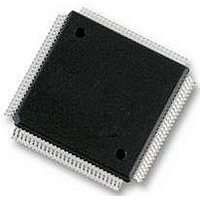
XC68HC12A0CPV8 Freescale Semiconductor, XC68HC12A0CPV8 Datasheet - Page 366

XC68HC12A0CPV8
Manufacturer Part Number
XC68HC12A0CPV8
Description
IC, 16BIT MCU, 68HC12, 8MHZ, TQFP-112
Manufacturer
Freescale Semiconductor
Datasheet
1.MC912D60ACFUE8.pdf
(460 pages)
Specifications of XC68HC12A0CPV8
Controller Family/series
68HC12
No. Of I/o's
68
Eeprom Memory Size
1KB
Ram Memory Size
2KB
Cpu Speed
8MHz
No. Of Timers
1
Core Size
16 Bit
Program Memory Size
60KB
Peripherals
ADC
Lead Free Status / RoHS Status
Lead free / RoHS Compliant
- Current page: 366 of 460
- Download datasheet (5Mb)
ATD0CTL5/ATD1CTL5 — ATD Control Register 5
Analog-to-Digital Converter
18.9.4 ATDCTL5 ATD Control Register 5
Technical Data
366
RESET:
Bit 7
0
0
S8C
6
0
ATD control register 5 determines the type of conversion sequence and
the analog input channels sampled. All writes to this register have an
immediate effect. If a conversion is in progress, the entire conversion
sequence is aborted. A write to this register (or ATDCTL4) initiates a new
conversion sequence (SCF and CCF bits are reset).
S8C / S1C — Conversion Sequence Length
1. Maximum conversion frequency is 2 MHz. Maximum PCLK divisor value will become
2. Minimum conversion frequency is 500 kHz. Minimum PCLK divisor value will become
S8C: Bit Position: 6, ATDCTL5
S1C: Bit Position: 3, ATDCTL3
The S8C/S1C bits define the length of a conversion sequence.
18-6
Prescale
maximum conversion rate that can be used on this ATD module.
minimum conversion rate that this ATD can perform.
00000
00001
00010
00011
00100
00101
00110
00111
Value
01xxx
1xxxx
SCAN
lists the coding combinations.
5
0
Analog-to-Digital Converter
Total Divisor
MULT
Table 18-5. Clock Prescaler Values
4
0
÷10
÷12
÷14
÷16
÷2
÷4
÷6
÷8
SC
3
0
Max PCLK
4 MHz
8 MHz
8 MHz
8 MHz
8 MHz
8 MHz
8 MHz
8 MHz
CC
Do Not Use
2
0
(1)
MC68HC912D60A — Rev. 3.1
CB
1
0
Freescale Semiconductor
Min PCLK
Bit 0
CA
1 MHz
2 MHz
3 MHz
4 MHz
5 MHz
6 MHz
7 MHz
8 MHz
0
$0065/$01E5
(2)
Table
Related parts for XC68HC12A0CPV8
Image
Part Number
Description
Manufacturer
Datasheet
Request
R
Part Number:
Description:
Manufacturer:
Freescale Semiconductor, Inc
Datasheet:
Part Number:
Description:
Manufacturer:
Freescale Semiconductor, Inc
Datasheet:
Part Number:
Description:
Manufacturer:
Freescale Semiconductor, Inc
Datasheet:
Part Number:
Description:
Manufacturer:
Freescale Semiconductor, Inc
Datasheet:
Part Number:
Description:
Manufacturer:
Freescale Semiconductor, Inc
Datasheet:
Part Number:
Description:
Manufacturer:
Freescale Semiconductor, Inc
Datasheet:
Part Number:
Description:
Manufacturer:
Freescale Semiconductor, Inc
Datasheet:
Part Number:
Description:
Manufacturer:
Freescale Semiconductor, Inc
Datasheet:
Part Number:
Description:
Manufacturer:
Freescale Semiconductor, Inc
Datasheet:
Part Number:
Description:
Manufacturer:
Freescale Semiconductor, Inc
Datasheet:
Part Number:
Description:
Manufacturer:
Freescale Semiconductor, Inc
Datasheet:
Part Number:
Description:
Manufacturer:
Freescale Semiconductor, Inc
Datasheet:
Part Number:
Description:
Manufacturer:
Freescale Semiconductor, Inc
Datasheet:
Part Number:
Description:
Manufacturer:
Freescale Semiconductor, Inc
Datasheet:
Part Number:
Description:
Manufacturer:
Freescale Semiconductor, Inc
Datasheet:


