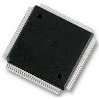
XC68HC12A0CPV8 Freescale Semiconductor, XC68HC12A0CPV8 Datasheet - Page 374

XC68HC12A0CPV8
Manufacturer Part Number
XC68HC12A0CPV8
Description
IC, 16BIT MCU, 68HC12, 8MHZ, TQFP-112
Manufacturer
Freescale Semiconductor
Datasheet
1.MC912D60ACFUE8.pdf
(460 pages)
Specifications of XC68HC12A0CPV8
Controller Family/series
68HC12
No. Of I/o's
68
Eeprom Memory Size
1KB
Ram Memory Size
2KB
Cpu Speed
8MHz
No. Of Timers
1
Core Size
16 Bit
Program Memory Size
60KB
Peripherals
ADC
Lead Free Status / RoHS Status
Lead free / RoHS Compliant
- Current page: 374 of 460
- Download datasheet (5Mb)
ATD0TESTL/ATD1TESTL — ATD Test Register
ATD0TESTH/ATD1TESTH — ATD Test Register
Analog-to-Digital Converter
18.9.6 ATDTEST Module Test Register (ATDTEST)
Technical Data
374
RESET:
RESET:
SAR1
SAR9
Bit 7
Bit 7
0
0
SAR0
SAR8
6
0
6
0
The test registers implement various special (test) modes used to test
the ATD module. The reset bit in ATDTEST1 is always read/write. The
SAR (successive approximation register) can always be read but only
written in special (test) mode.
The functions implemented by the test registers are reserved for factory
test.
SAR[9:0] — Successive Approximation Register
RST — Test Mode Reset Bit
This ten bit value represents the contents of the AD machine’s
successive approximation register. This value can always be read. It
can only be written in special (test) mode. Note that ATDTEST0 acts
as a ten bit register since the entire SAR is read/written when
accessing this address.
When set, this bit causes the ATD module to reset itself. This sets all
registers to their reset state (note the reset state of the reset bit is
zero), the current conversion and conversion sequence are aborted,
pending interrupts are cleared, and the module is placed in an idle
mode.
0 = No reset
1 = Reset the ATD module
SAR7
RST
5
0
5
0
Analog-to-Digital Converter
SAR6
4
0
4
0
0
SAR5
3
0
3
0
0
SAR4
2
0
2
0
0
SAR3
MC68HC912D60A — Rev. 3.1
1
0
1
0
0
Freescale Semiconductor
SAR2
Bit 0
Bit 0
0
0
0
$0069/$01E9
$0068/$01E8
Related parts for XC68HC12A0CPV8
Image
Part Number
Description
Manufacturer
Datasheet
Request
R
Part Number:
Description:
Manufacturer:
Freescale Semiconductor, Inc
Datasheet:
Part Number:
Description:
Manufacturer:
Freescale Semiconductor, Inc
Datasheet:
Part Number:
Description:
Manufacturer:
Freescale Semiconductor, Inc
Datasheet:
Part Number:
Description:
Manufacturer:
Freescale Semiconductor, Inc
Datasheet:
Part Number:
Description:
Manufacturer:
Freescale Semiconductor, Inc
Datasheet:
Part Number:
Description:
Manufacturer:
Freescale Semiconductor, Inc
Datasheet:
Part Number:
Description:
Manufacturer:
Freescale Semiconductor, Inc
Datasheet:
Part Number:
Description:
Manufacturer:
Freescale Semiconductor, Inc
Datasheet:
Part Number:
Description:
Manufacturer:
Freescale Semiconductor, Inc
Datasheet:
Part Number:
Description:
Manufacturer:
Freescale Semiconductor, Inc
Datasheet:
Part Number:
Description:
Manufacturer:
Freescale Semiconductor, Inc
Datasheet:
Part Number:
Description:
Manufacturer:
Freescale Semiconductor, Inc
Datasheet:
Part Number:
Description:
Manufacturer:
Freescale Semiconductor, Inc
Datasheet:
Part Number:
Description:
Manufacturer:
Freescale Semiconductor, Inc
Datasheet:
Part Number:
Description:
Manufacturer:
Freescale Semiconductor, Inc
Datasheet:


