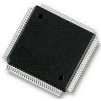
XC68HC12A0CPV8 Freescale Semiconductor, XC68HC12A0CPV8 Datasheet - Page 48

XC68HC12A0CPV8
Manufacturer Part Number
XC68HC12A0CPV8
Description
IC, 16BIT MCU, 68HC12, 8MHZ, TQFP-112
Manufacturer
Freescale Semiconductor
Datasheet
1.MC912D60ACFUE8.pdf
(460 pages)
Specifications of XC68HC12A0CPV8
Controller Family/series
68HC12
No. Of I/o's
68
Eeprom Memory Size
1KB
Ram Memory Size
2KB
Cpu Speed
8MHz
No. Of Timers
1
Core Size
16 Bit
Program Memory Size
60KB
Peripherals
ADC
Lead Free Status / RoHS Status
Lead free / RoHS Compliant
- Current page: 48 of 460
- Download datasheet (5Mb)
Pinout and Signal Descriptions
3.5.6 Mode Select (SMODN, MODA, and MODB)
3.5.7 Single-Wire Background Mode Pin (BKGD)
3.5.8 External Address and Data Buses (ADDR[15:0] and DATA[15:0])
Technical Data
48
The state of these pins during reset determine the MCU operating mode.
After reset, MODA and MODB can be configured as instruction queue
tracking signals IPIPE0 and IPIPE1. MODA and MODB have active pull-
downs during reset.
The SMODN pin has an active pull-up when configured as input. This pin
can be used as BKGD or TAGHI after reset.
The BKGD pin receives and transmits serial background debugging
commands. A special self-timing protocol is used. The BKGD pin has an
active pull-up when configured as input; BKGD has no pull-up control.
Refer to
External bus pins share function with general-purpose I/O ports A and B.
In single-chip operating modes, the pins can be used for I/O; in
expanded modes, the pins are used for the external buses.
In expanded wide mode, ports A and B are used for multiplexed 16-bit
data and address buses. PA[7:0] correspond to
ADDR[15:8]/DATA[15:8]; PB[7:0] correspond to ADDR[7:0]/DATA[7:0].
In expanded narrow mode, ports A and B are used for the16-bit address
bus, and an 8-bit data bus is multiplexed with the most significant half of
the address bus on port A. In this mode, 16-bit data is handled as two
back-to-back bus cycles, one for the high byte followed by one for the
low byte. PA[7:0] correspond to ADDR[15:8] and to DATA[15:8] or
DATA[7:0], depending on the bus cycle. The state of the address pin
should be latched at the rising edge of E. To allow for maximum address
setup time at external devices, a transparent latch should be used.
Development
Pinout and Signal Descriptions
Support.
MC68HC912D60A — Rev. 3.1
Freescale Semiconductor
Related parts for XC68HC12A0CPV8
Image
Part Number
Description
Manufacturer
Datasheet
Request
R
Part Number:
Description:
Manufacturer:
Freescale Semiconductor, Inc
Datasheet:
Part Number:
Description:
Manufacturer:
Freescale Semiconductor, Inc
Datasheet:
Part Number:
Description:
Manufacturer:
Freescale Semiconductor, Inc
Datasheet:
Part Number:
Description:
Manufacturer:
Freescale Semiconductor, Inc
Datasheet:
Part Number:
Description:
Manufacturer:
Freescale Semiconductor, Inc
Datasheet:
Part Number:
Description:
Manufacturer:
Freescale Semiconductor, Inc
Datasheet:
Part Number:
Description:
Manufacturer:
Freescale Semiconductor, Inc
Datasheet:
Part Number:
Description:
Manufacturer:
Freescale Semiconductor, Inc
Datasheet:
Part Number:
Description:
Manufacturer:
Freescale Semiconductor, Inc
Datasheet:
Part Number:
Description:
Manufacturer:
Freescale Semiconductor, Inc
Datasheet:
Part Number:
Description:
Manufacturer:
Freescale Semiconductor, Inc
Datasheet:
Part Number:
Description:
Manufacturer:
Freescale Semiconductor, Inc
Datasheet:
Part Number:
Description:
Manufacturer:
Freescale Semiconductor, Inc
Datasheet:
Part Number:
Description:
Manufacturer:
Freescale Semiconductor, Inc
Datasheet:
Part Number:
Description:
Manufacturer:
Freescale Semiconductor, Inc
Datasheet:


