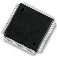
XC68HC12A0CPV8 Freescale Semiconductor, XC68HC12A0CPV8 Datasheet - Page 58

XC68HC12A0CPV8
Manufacturer Part Number
XC68HC12A0CPV8
Description
IC, 16BIT MCU, 68HC12, 8MHZ, TQFP-112
Manufacturer
Freescale Semiconductor
Datasheet
1.MC912D60ACFUE8.pdf
(460 pages)
Specifications of XC68HC12A0CPV8
Controller Family/series
68HC12
No. Of I/o's
68
Eeprom Memory Size
1KB
Ram Memory Size
2KB
Cpu Speed
8MHz
No. Of Timers
1
Core Size
16 Bit
Program Memory Size
60KB
Peripherals
ADC
Lead Free Status / RoHS Status
Lead free / RoHS Compliant
- Current page: 58 of 460
- Download datasheet (5Mb)
Pinout and Signal Descriptions
3.6.10 Port S
3.6.11 Port T
Technical Data
58
Port S is the 8-bit interface to the standard serial interface consisting of
the two serial communications interfaces (SCI1 and SCI0) and the serial
peripheral interface (SPI) subsystems. Port S pins are available for
general-purpose parallel I/O when standard serial functions are not
enabled.
Port S pins serve several functions depending on the various internal
control registers. If WOMS bit in the SC0CR1register is set, the P-
channel drivers of the output buffers are disabled for bits 0 through 1 for
the SCSI1 (2 through 3 for the SCI0). If SWOM bit in the SP0CR1
register is set, the P-channel drivers of the output buffers are disabled
for bits 4 through 7 (wire-ORed mode). The open drain control effects to
both the serial and the general-purpose outputs. If the RDPSx bits in the
PURDS register are set, the appropriate Port S pin drive capabilities are
reduced. If PUPSx bits in the PURDS register are set, the appropriate
pull-up device is connected to each port S pin which is programmed as
a general-purpose input. If the pin is programmed as a general-purpose
output, the pull-up is disconnected from the pin regardless of the state of
the individual PUPSx bits. See
This port provides eight general-purpose I/O pins when not enabled for
input capture and output compare in the timer and pulse accumulator
subsystem. The TEN bit in the TSCR register enables the timer function.
The pulse accumulator subsystem is enabled with the PAEN bit in the
PACTL register.
Register DDRT determines pin direction of port T when used for general-
purpose I/O. When DDRT bits are set, the corresponding pin is
configured for output. On reset the DDRT bits are cleared and the
corresponding pin is configured for input.
When the PUPT bit in the TMSK2 register is set, all input pins are pulled
up internally by an active pull-up device. Pull-ups are disabled after
reset.
Pinout and Signal Descriptions
Multiple Serial
MC68HC912D60A — Rev. 3.1
Interface.
Freescale Semiconductor
Related parts for XC68HC12A0CPV8
Image
Part Number
Description
Manufacturer
Datasheet
Request
R
Part Number:
Description:
Manufacturer:
Freescale Semiconductor, Inc
Datasheet:
Part Number:
Description:
Manufacturer:
Freescale Semiconductor, Inc
Datasheet:
Part Number:
Description:
Manufacturer:
Freescale Semiconductor, Inc
Datasheet:
Part Number:
Description:
Manufacturer:
Freescale Semiconductor, Inc
Datasheet:
Part Number:
Description:
Manufacturer:
Freescale Semiconductor, Inc
Datasheet:
Part Number:
Description:
Manufacturer:
Freescale Semiconductor, Inc
Datasheet:
Part Number:
Description:
Manufacturer:
Freescale Semiconductor, Inc
Datasheet:
Part Number:
Description:
Manufacturer:
Freescale Semiconductor, Inc
Datasheet:
Part Number:
Description:
Manufacturer:
Freescale Semiconductor, Inc
Datasheet:
Part Number:
Description:
Manufacturer:
Freescale Semiconductor, Inc
Datasheet:
Part Number:
Description:
Manufacturer:
Freescale Semiconductor, Inc
Datasheet:
Part Number:
Description:
Manufacturer:
Freescale Semiconductor, Inc
Datasheet:
Part Number:
Description:
Manufacturer:
Freescale Semiconductor, Inc
Datasheet:
Part Number:
Description:
Manufacturer:
Freescale Semiconductor, Inc
Datasheet:
Part Number:
Description:
Manufacturer:
Freescale Semiconductor, Inc
Datasheet:


