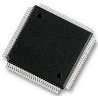
XC68HC12A0CPV8 Freescale Semiconductor, XC68HC12A0CPV8 Datasheet - Page 99

XC68HC12A0CPV8
Manufacturer Part Number
XC68HC12A0CPV8
Description
IC, 16BIT MCU, 68HC12, 8MHZ, TQFP-112
Manufacturer
Freescale Semiconductor
Datasheet
1.MC912D60ACFUE8.pdf
(460 pages)
Specifications of XC68HC12A0CPV8
Controller Family/series
68HC12
No. Of I/o's
68
Eeprom Memory Size
1KB
Ram Memory Size
2KB
Cpu Speed
8MHz
No. Of Timers
1
Core Size
16 Bit
Program Memory Size
60KB
Peripherals
ADC
Lead Free Status / RoHS Status
Lead free / RoHS Compliant
- Current page: 99 of 460
- Download datasheet (5Mb)
FEE32LCK/FEE28LCK — Flash EEPROM Lock Control Register
FEE32MCR/FEE28MCR — Flash EEPROM Module Configuration Register
FEE32CTL/FEE28CTL — Flash EEPROM Control Register
7.6 Flash EEPROM Registers
MC68HC912D60A — Rev. 3.1
Freescale Semiconductor
RESET:
RESET:
RESET:
Bit 7
Bit 7
Bit 7
0
0
0
0
0
0
6
0
0
6
0
0
6
0
0
LOCK — Lock Register Bit
This register controls the operation of the Flash EEPROM array. BOOTP
cannot be changed when the LOCK control bit in the FEELCK register is
set or if HVEN or PGM or ERAS in the FEECTL register is set .
BOOTP — Boot Protect
This register controls the programming and erasure of the Flash
EEPROM.
In normal modes the LOCK bit can only be written once after reset.
The boot blocks are located at $6000–$7FFF and $E000–$FFFF for
each Flash EEPROM module.
0 = Enable write to FEEMCR register
1 = Disable write to FEEMCR register
0 = Enable erase and program of 8K byte boot block
1 = Disable erase and program of 8K byte boot block
5
0
0
5
0
0
5
0
0
FEESWAI
Flash Memory
4
0
0
4
0
0
4
0
HVEN
3
0
3
0
0
3
0
0
2
0
0
2
0
0
2
0
0
ERAS
1
0
1
0
0
1
0
0
Flash EEPROM Registers
BOOTP
LOCK
PGM
Bit 0
Bit 0
Bit 0
0
0
1
Technical Data
Flash Memory
$00F4/$00F8
$00F5/$00F9
$00F7/$00FB
99
Related parts for XC68HC12A0CPV8
Image
Part Number
Description
Manufacturer
Datasheet
Request
R
Part Number:
Description:
Manufacturer:
Freescale Semiconductor, Inc
Datasheet:
Part Number:
Description:
Manufacturer:
Freescale Semiconductor, Inc
Datasheet:
Part Number:
Description:
Manufacturer:
Freescale Semiconductor, Inc
Datasheet:
Part Number:
Description:
Manufacturer:
Freescale Semiconductor, Inc
Datasheet:
Part Number:
Description:
Manufacturer:
Freescale Semiconductor, Inc
Datasheet:
Part Number:
Description:
Manufacturer:
Freescale Semiconductor, Inc
Datasheet:
Part Number:
Description:
Manufacturer:
Freescale Semiconductor, Inc
Datasheet:
Part Number:
Description:
Manufacturer:
Freescale Semiconductor, Inc
Datasheet:
Part Number:
Description:
Manufacturer:
Freescale Semiconductor, Inc
Datasheet:
Part Number:
Description:
Manufacturer:
Freescale Semiconductor, Inc
Datasheet:
Part Number:
Description:
Manufacturer:
Freescale Semiconductor, Inc
Datasheet:
Part Number:
Description:
Manufacturer:
Freescale Semiconductor, Inc
Datasheet:
Part Number:
Description:
Manufacturer:
Freescale Semiconductor, Inc
Datasheet:
Part Number:
Description:
Manufacturer:
Freescale Semiconductor, Inc
Datasheet:
Part Number:
Description:
Manufacturer:
Freescale Semiconductor, Inc
Datasheet:


