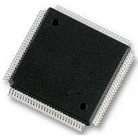
XC68HC12A0CPV8 Freescale Semiconductor, XC68HC12A0CPV8 Datasheet - Page 57

XC68HC12A0CPV8
Manufacturer Part Number
XC68HC12A0CPV8
Description
IC, 16BIT MCU, 68HC12, 8MHZ, TQFP-112
Manufacturer
Freescale Semiconductor
Datasheet
1.MC912D60ACFUE8.pdf
(460 pages)
Specifications of XC68HC12A0CPV8
Controller Family/series
68HC12
No. Of I/o's
68
Eeprom Memory Size
1KB
Ram Memory Size
2KB
Cpu Speed
8MHz
No. Of Timers
1
Core Size
16 Bit
Program Memory Size
60KB
Peripherals
ADC
Lead Free Status / RoHS Status
Lead free / RoHS Compliant
- Current page: 57 of 460
- Download datasheet (5Mb)
3.6.8 Port AD0
3.6.9 Port P
MC68HC912D60A — Rev. 3.1
Freescale Semiconductor
Port AD1 pins are inputs; no data direction register is associated with this
port. The port has no resistive input loads and no reduced drive controls.
Refer to
Port AD1 is not available in the 80-pin package.
Input to the analog-to-digital subsystem and general-purpose input.
When analog-to-digital functions are not enabled, the port has eight
general-purpose input pins, PAD0[7:0]. The ADPU bit in the ATD0CTL2
register enables the A/D function.
Port AD0 pins are inputs; no data direction register is associated with this
port. The port has no resistive input loads and no reduced drive controls.
Refer to
The four pulse-width modulation channel outputs share general-purpose
port P pins. The PWM function is enabled with the PWEN register.
Enabling PWM pins takes precedence over the general-purpose port.
When pulse-width modulation is not in use, the port pins may be used for
general-purpose I/O.
Register DDRP determines pin direction of port P when used for
general-purpose I/O. When DDRP bits are set, the corresponding pin is
configured for output. On reset the DDRP bits are cleared and the
corresponding pin is configured for input.
When the PUPP bit in the PWCTL register is set, all input pins are pulled
up internally by an active pull-up device. Pull-ups are disabled after
reset.
Setting the RDPP bit in the PWCTL register configures all port P outputs
to have reduced drive levels. Levels are at normal drive capability after
reset. The PWCTL register can be read or written anytime after reset.
Refer to
Analog-to-Digital
Analog-to-Digital
Pulse Width
Pinout and Signal Descriptions
Modulator.
Converter.
Converter.
Pinout and Signal Descriptions
Technical Data
Port Signals
57
Related parts for XC68HC12A0CPV8
Image
Part Number
Description
Manufacturer
Datasheet
Request
R
Part Number:
Description:
Manufacturer:
Freescale Semiconductor, Inc
Datasheet:
Part Number:
Description:
Manufacturer:
Freescale Semiconductor, Inc
Datasheet:
Part Number:
Description:
Manufacturer:
Freescale Semiconductor, Inc
Datasheet:
Part Number:
Description:
Manufacturer:
Freescale Semiconductor, Inc
Datasheet:
Part Number:
Description:
Manufacturer:
Freescale Semiconductor, Inc
Datasheet:
Part Number:
Description:
Manufacturer:
Freescale Semiconductor, Inc
Datasheet:
Part Number:
Description:
Manufacturer:
Freescale Semiconductor, Inc
Datasheet:
Part Number:
Description:
Manufacturer:
Freescale Semiconductor, Inc
Datasheet:
Part Number:
Description:
Manufacturer:
Freescale Semiconductor, Inc
Datasheet:
Part Number:
Description:
Manufacturer:
Freescale Semiconductor, Inc
Datasheet:
Part Number:
Description:
Manufacturer:
Freescale Semiconductor, Inc
Datasheet:
Part Number:
Description:
Manufacturer:
Freescale Semiconductor, Inc
Datasheet:
Part Number:
Description:
Manufacturer:
Freescale Semiconductor, Inc
Datasheet:
Part Number:
Description:
Manufacturer:
Freescale Semiconductor, Inc
Datasheet:
Part Number:
Description:
Manufacturer:
Freescale Semiconductor, Inc
Datasheet:


