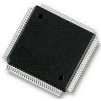
XC68HC12A0CPV8 Freescale Semiconductor, XC68HC12A0CPV8 Datasheet - Page 78

XC68HC12A0CPV8
Manufacturer Part Number
XC68HC12A0CPV8
Description
IC, 16BIT MCU, 68HC12, 8MHZ, TQFP-112
Manufacturer
Freescale Semiconductor
Datasheet
1.MC912D60ACFUE8.pdf
(460 pages)
Specifications of XC68HC12A0CPV8
Controller Family/series
68HC12
No. Of I/o's
68
Eeprom Memory Size
1KB
Ram Memory Size
2KB
Cpu Speed
8MHz
No. Of Timers
1
Core Size
16 Bit
Program Memory Size
60KB
Peripherals
ADC
Lead Free Status / RoHS Status
Lead free / RoHS Compliant
- Current page: 78 of 460
- Download datasheet (5Mb)
Operating Modes and Resource Mapping
5.5.1 Register Block Mapping
INITRG — Initialization of Internal Register Position Register
Technical Data
78
RESET:
REG15
Bit 7
0
REG14
6
0
data. It is made of the 28K byte FEE28 array mapped from $1000 to
$7FFF at reset and of the 32 K byte FEE32 array mapped from $8000 to
$FFFF at reset. MAPROM bit in the MISC register allows the swapping
of the two flash arrays.
After reset the 512 byte register block resides at location $0000 but can
be reassigned to any 2K byte boundary within the standard 64K byte
address space. Mapping of internal registers is controlled by five bits in
the INITRG register. The register block occupies the first 512 bytes of the
2K byte block.
REG[15:11] — Internal register map position
These bits specify the upper five bits of the 16-bit registers address.
Normal modes: write once; special modes: write anytime. Read
anytime.
Operating Modes and Resource Mapping
REG13
5
0
Precedence
1
2
3
4
5
6
REG12
4
0
Table 5-2. Mapping Precedence
On-Chip Flash EEPROM (MC68HC912D60A)
REG11
3
0
BDM ROM (if active)
External Memory
Register Space
2
0
0
Resource
EEPROM
RAM
MC68HC912D60A — Rev. 3.1
1
0
0
Freescale Semiconductor
MMSWAI
Bit 0
0
$0011
Related parts for XC68HC12A0CPV8
Image
Part Number
Description
Manufacturer
Datasheet
Request
R
Part Number:
Description:
Manufacturer:
Freescale Semiconductor, Inc
Datasheet:
Part Number:
Description:
Manufacturer:
Freescale Semiconductor, Inc
Datasheet:
Part Number:
Description:
Manufacturer:
Freescale Semiconductor, Inc
Datasheet:
Part Number:
Description:
Manufacturer:
Freescale Semiconductor, Inc
Datasheet:
Part Number:
Description:
Manufacturer:
Freescale Semiconductor, Inc
Datasheet:
Part Number:
Description:
Manufacturer:
Freescale Semiconductor, Inc
Datasheet:
Part Number:
Description:
Manufacturer:
Freescale Semiconductor, Inc
Datasheet:
Part Number:
Description:
Manufacturer:
Freescale Semiconductor, Inc
Datasheet:
Part Number:
Description:
Manufacturer:
Freescale Semiconductor, Inc
Datasheet:
Part Number:
Description:
Manufacturer:
Freescale Semiconductor, Inc
Datasheet:
Part Number:
Description:
Manufacturer:
Freescale Semiconductor, Inc
Datasheet:
Part Number:
Description:
Manufacturer:
Freescale Semiconductor, Inc
Datasheet:
Part Number:
Description:
Manufacturer:
Freescale Semiconductor, Inc
Datasheet:
Part Number:
Description:
Manufacturer:
Freescale Semiconductor, Inc
Datasheet:
Part Number:
Description:
Manufacturer:
Freescale Semiconductor, Inc
Datasheet:


