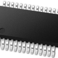
PIC24FJ64GB002-I/SS Microchip Technology, PIC24FJ64GB002-I/SS Datasheet - Page 131

PIC24FJ64GB002-I/SS
Manufacturer Part Number
PIC24FJ64GB002-I/SS
Description
16-bit, 16 MIPS, 64KB Flash, 8KB RAM, Nanowatt XLP, USB OTG 28 SSOP .209in TUBE
Manufacturer
Microchip Technology
Specifications of PIC24FJ64GB002-I/SS
Processor Series
PIC24
Core
PIC24F
Data Bus Width
16 bit
Program Memory Type
Flash
Program Memory Size
64 KB
Data Ram Size
8192 B
Interface Type
I2C, SPI, UART
Maximum Clock Frequency
32 MHz
Number Of Programmable I/os
21
Number Of Timers
5
Operating Supply Voltage
2 V to 3.6 V
Maximum Operating Temperature
+ 85 C
Mounting Style
SMD/SMT
Package / Case
SSOP-28
Development Tools By Supplier
MPLAB Integrated Development Environment
Minimum Operating Temperature
- 40 C
Operating Temperature Range
- 40 C to + 85 C
Supply Current (max)
300 mA
Lead Free Status / Rohs Status
Lead free / RoHS Compliant
Available stocks
Company
Part Number
Manufacturer
Quantity
Price
Part Number:
PIC24FJ64GB002-I/SS
Manufacturer:
MICROCHIP/微芯
Quantity:
20 000
- Current page: 131 of 352
- Download datasheet (3Mb)
10.4.3.2
In contrast to inputs, the outputs of the Peripheral Pin
Select options are mapped on the basis of the pin. In
this case, a control register associated with a particular
pin dictates the peripheral output to be mapped. The
RPORx registers are used to control output mapping.
Each register contains up to two 5-bit fields, with each
field being associated with one RPn pin (see
Register 10-15 through Register 10-27). The value of
TABLE 10-3:
2010 Microchip Technology Inc.
Note 1:
Output Function Number
2:
3:
Setting the RPORx register with the listed value assigns that output function to the associated RPn pin.
The NULL function is assigned to all RPn outputs at device Reset and disables the RPn output function.
IrDA
Output Mapping
®
23-28
SELECTABLE OUTPUT SOURCES (MAPS FUNCTION TO OUTPUT)
BCLK functionality uses this output.
10
11
12
18
19
20
21
22
29
30
31
0
1
2
3
4
5
6
7
8
9
(1)
PIC24FJ64GB004 FAMILY
SCK1OUT
SCK2OUT
Function
U1RTS
U2RTS
SS1OUT
SS2OUT
(unused)
(unused)
NULL
C1OUT
C2OUT
C3OUT
CTPLS
SDO1
SDO2
U1TX
U2TX
OC1
OC2
OC3
OC4
OC5
(2)
(3)
(3)
the bit field corresponds to one of the peripherals and
that peripheral’s output is mapped to the pin (see
Table 10-3).
Because of the mapping technique, the list of
peripherals for output mapping also includes a null value
of ‘000000’. This permits any given pin to remain dis-
connected from the output of any of the pin-selectable
peripherals.
UART1 Request To Send
UART2 Request To Send
SPI1 Slave Select Output
SPI2 Slave Select Output
Comparator 1 Output
Comparator 2 Output
Comparator 3 Output
CTMU Output Pulse
SPI1 Clock Output
Output Compare 1
Output Compare 2
Output Compare 3
Output Compare 4
Output Compare 5
SPI2 Clock Output
SPI1 Data Output
SPI2 Data Output
UART1 Transmit
UART2 Transmit
Output Name
Null
NC
NC
DS39940D-page 131
Related parts for PIC24FJ64GB002-I/SS
Image
Part Number
Description
Manufacturer
Datasheet
Request
R

Part Number:
Description:
Manufacturer:
Microchip Technology Inc.
Datasheet:

Part Number:
Description:
Manufacturer:
Microchip Technology Inc.
Datasheet:

Part Number:
Description:
Manufacturer:
Microchip Technology Inc.
Datasheet:

Part Number:
Description:
Manufacturer:
Microchip Technology Inc.
Datasheet:

Part Number:
Description:
Manufacturer:
Microchip Technology Inc.
Datasheet:

Part Number:
Description:
Manufacturer:
Microchip Technology Inc.
Datasheet:

Part Number:
Description:
Manufacturer:
Microchip Technology Inc.
Datasheet:

Part Number:
Description:
Manufacturer:
Microchip Technology Inc.
Datasheet:


